top of page


A Field-Centric Perspective on Charge and Energy Transfer in Classical Electromagnetism
Explore a field-centric view on energy transfer in classical electromagnetism. Discover how energy transfer insights challenge traditional paradigms.

Dario Fresu
4 min read


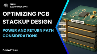
Optimizing PCB Stackup Design: Power and Return Path Considerations
Discover how to optimize PCB stackup for superior performance with insights on power and return path considerations. Master PCB stackup design today!

Dario Fresu
8 min read


EMC Filter Topologies: EMI Control Strategies in Electronics Design
Discover top EMC Filters strategies for electronics design. Learn about five key EMC Filters configurations to enhance EMI control in your systems.

Dario Fresu
7 min read


Understanding 90-Degree Bends in PCB Design: A Practical Guide
Explore the intricacies of pcb design with our practical guide on 90-degree bends. Master pcb design techniques for optimized performance.

Dario Fresu
8 min read


Redefining Current and Charge: A Field-Based Perspective on Electromagnetism
Explore a fresh perspective on Electromagnetism in our blog. Discover how Electromagnetism redefines current and charge through field dynamics.

Dario Fresu
11 min read


How to Effectively Conduct an EMI Design Review for Your PCB
In this article, I will guide you through the basics of conducting an EMI project review for a Printed Circuit Board layout.

Dario Fresu
23 min read


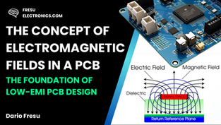
The concept of Electromagnetic Fields in a PCB
Explore the concept of fields in PCB and learn how to control electromagnetic fields in PCB design for low EMI. Master fields in PCB today!

Dario Fresu
6 min read


Why smart engineers fail EMC tests (it's not what you think)
Discover why smart engineers fail EMC tests and what you can do about it. Learn the secrets to mastering EMC tests and improving your designs.

Dario Fresu
7 min read


Effective Strategies for Managing EMI in PCBs with Low and High-Speed Signal Return Currents
Discover effective strategies for managing EMI in PCBs with High-Speed Signal return currents. Learn how High-Speed Signal behavior impacts PCB design.

Dario Fresu
8 min read


Power Planes as Return Reference Planes in PCB Design: Challenges and Solutions in Multilayer Stackups
Explore the challenges of using power planes as return reference planes in multilayer PCB design. Discover solutions for multilayer PCB efficiency.

Dario Fresu
6 min read


Mastering Electromagnetic Interference: Elevate Electronics with EMC Design
Explore how mastering Electromagnetic Interference can elevate electronics with EMC design. Learn to tackle Electromagnetic Interference effectively.

Dario Fresu
7 min read


Why ‘Ground’ Falls Short: A Call for a Clearer Term in Circuit Design
Discover why the term "ground" is misleading in Circuit Design and explore strategies for achieving reliable performance in Circuit Design.

Dario Fresu
6 min read


Radiated Emissions Testing and the Role of EMC Current Clamps
Discover how EMC current clamps can help you estimate radiated emissions effectively. Learn how radiated emissions impact EMC compliance.

Dario Fresu
7 min read


Understanding EN 61000-4-6: A Key Standard for Conducted RF Immunity in EMC Design
Explore the significance of EN 61000-4-6 in EMC design. Learn how EN 61000-4-6 ensures robust electronic systems against RF interference.

Dario Fresu
6 min read


How Return Reference Planes Impact EMI Control in PCB Design
Discover how return reference planes are crucial for effective EMI Control in PCB design. Learn essential strategies for EMI Control today.

Dario Fresu
6 min read


The Essentials of Electromagnetic Compatibility Training
Discover the importance of Electromagnetic Compatibility Training in ensuring device reliability and compliance.

Dario Fresu
4 min read


The Pitfalls of Overreliance on Post-Design Fixes in Electromagnetic Compatibility Compliance
Explore the pitfalls of overreliance on post-design fixes in Electromagnetic Compatibility compliance.

Dario Fresu
6 min read


Mastering PCB Design with IPC-2221: The Industry’s Foundational Standard
Unlock the secrets of PCB design with IPC-2221, the industry's foundational standard. Discover how IPC-2221 can enhance your design skills.

Dario Fresu
4 min read


Signal Integrity: The Key to EMC Compliance for Electronic Engineers
Consider this scenario: You're an electronic engineer nearing the completion of a product design. After months of meticulous...

Dario Fresu
8 min read


Why EMI Keeps Ruining Your PCB Designs (And What to Do Before It’s Too Late)
Discover why EMI keeps disrupting your PCB designs and learn how to tackle EMI issues effectively before it's too late.

Dario Fresu
7 min read


Optimizing PCB Layout for EMI Control: Managing Fast-Changing Currents
Designing printed circuit boards (PCBs) requires more than following basic guidelines; it demands a deep understanding of physics ...

Dario Fresu
7 min read


Mastering Input Filter Design: Achieving EMC Compliance for Power Converters
This article delves into the strategic role of input filters, their influence on closed-loop dynamics.

Dario Fresu
4 min read


Mastering PCB Design: Tips for Beginners
In this blog post, we will explore practical tips for beginners in PCB design, review essential tools, and provide insights on how to ...

Fresu Electronics AI
4 min read


Your First Steps in PCB Design: A Beginner’s Guide
Master PCB design with this beginner’s guide—learn key terms, pick software like KiCad, and start creating with confidence!

Fresu Electronics AI
5 min read
Fresu Electronics Newsletter
bottom of page

