

Why ‘Ground’ Falls Short: A Call for a Clearer Term in Circuit Design
- Dario Fresu

- Apr 17, 2025
- 6 min read
Updated: Apr 21, 2025
The term “ground” is a cornerstone of electronics, appearing in circuit schematics, textbooks, and engineering discussions. However, it is a misleading label that oversimplifies the role of the return and reference conductor—the critical pathway that carries current back to its source along the route of least impedance. This misconception can lead to design errors that impair circuit performance, spanning analog circuits to high-speed digital systems. By exploring the historical origins of “ground,” examining current flow dynamics, and presenting practical design strategies, this article demonstrates why “ground” is an inadequate term and advocates focusing on the path of least impedance to achieve reliable circuit performance.

The Story Behind "Ground"
In the early days of telegraphy, engineers tackled the challenge of transmitting signals over vast distances. They discovered an innovative solution: instead of using two wires, they could leverage the earth as a conductor. By burying metal plates in the soil, they enabled currents to flow through the ground, reducing costs and labor. This breakthrough gave rise to the term “ground,” suggesting electricity could seamlessly sink into the earth.
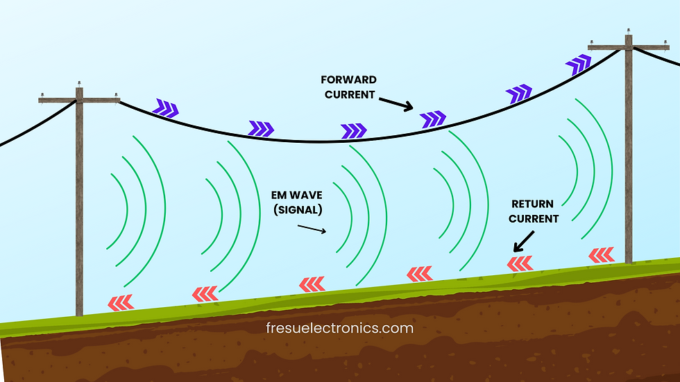
However, this approach had limitations. As urban areas expanded, electric trams and other machinery introduced electromagnetic interference, disrupting telegraph signals. Engineers adapted, often reverting to metallic conductors to ensure signal clarity. This history established “ground” as a convenient shorthand, but it perpetuated a flawed notion: that “ground” is a universal, ideal conductor. Today, the term is applied to various circuit functions, causing confusion across designs, from simple battery-powered devices to sophisticated electronic systems.
Why "Ground" Doesn’t Work in Circuit Design
The term “ground” implies a singular, ideal point of zero potential, but in practice, the conductor labeled “ground” serves as a dynamic return and reference plane, managing current flow and signal reference. Its behavior varies with circuit conditions, rendering “ground” an oversimplified and misleading label.
Many Roles, One Name
The confusion surrounding “ground” stems from its use to describe distinct functions, each with unique electrical characteristics:
Signal Reference: A low-impedance plane or trace that establishes the voltage reference for signals.
Power Return: The pathway for DC or AC power currents returning to the source.
Safety Earth: A physical connection to the earth for safety in AC power systems.
Chassis Shield: A conductive enclosure serving as a reference for EMI shielding or cable connections.
These functions are not interchangeable. At low frequencies, their differences may be manageable, but at higher frequencies—typically above 1 MHz—the impedance of these paths, influenced by inductance, can cause voltage drops, common-mode currents, signal degradation, and electromagnetic interference (EMI). The term “ground” obscures these complexities, fostering the erroneous assumption that all “grounds” are equivalent and ideal.
No Perfect Conductor
The notion of “ground” as an ideal, zero-potential conductor is a misconception. All conductors exhibit resistance and inductance, affecting current flow. For instance, a 30 cm × 30 cm copper plate used as a return path may have an impedance of approximately 0.25 ohms at high frequencies, resulting in a 2.5-millivolt voltage drop for a 10-milliamp current—far from the “zero” implied by “ground.” Even in basic circuits, a conductor labeled “ground” can introduce voltage differences that degrade performance, such as distorting a signal. The term “ground” misleads by ignoring these practical limitations.
Current Flow: The Path of Least Impedance
To understand why “ground” is inadequate, we must examine the principles governing current flow. Kirchhoff’s Current Law mandates that current returns to its source, forming a closed loop with no possibility of vanishing into a sink. Maxwell’s equations reinforce this, showing that circuits maintain continuous loops through conduction current (in conductors) and displacement current (through dielectrics, such as a circuit board’s insulating substrate). The current’s path is determined by impedance—the total opposition to flow, comprising resistance and inductance.
Low-Frequency Behavior: Resistance Rules
At low frequencies, resistance is the primary component of impedance, and current follows the path of least resistance, spreading through the conductor surface, and often the shortest route. Consider a printed circuit board (PCB) with a signal trace over a return and reference plane (RRP):
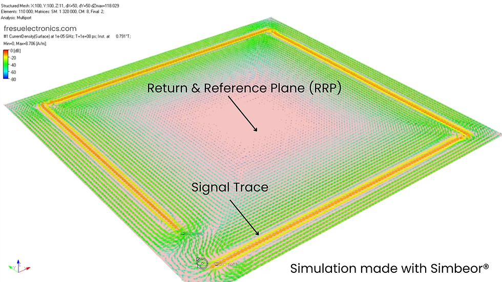
For a 10 kHz signal, the return current occupies most of the plane's surface. The plane's low resistance provides an efficient return path, consistent with the intuitive concept of "ground" as a dependable conductor.
High-Frequency Behavior: Inductance Dominates
At higher frequencies, inductance dominates impedance, increasing with signal speed, and current seeks the path of least inductance, typically forming a smaller loop, even if longer. In the same PCB:
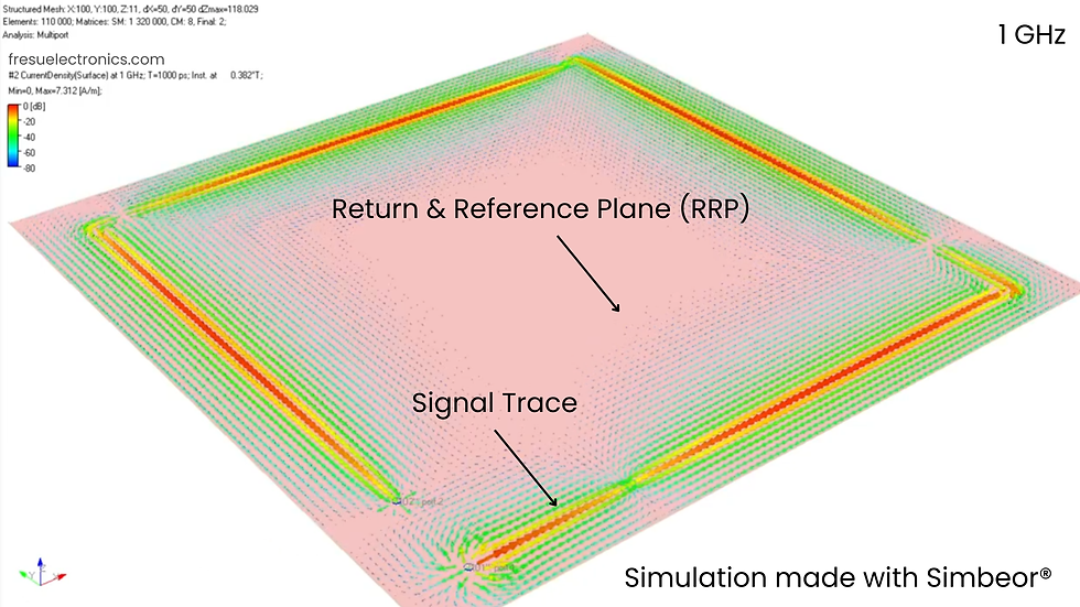
For a 1 GHz signal, the return current flows closely beneath the trace, minimizing the loop area. This shift from resistance to inductance dominance typically occurs between 10 kHz and 1 MHz, depending on circuit geometry. A 20 cm trace with a large loop may have significantly higher inductance than a tight loop, highlighting why “ground” fails to describe the dynamic return path.
The Hidden Schematic: Parasitic Effects
The term “ground” overlooks parasitic effects, which complicate return paths. Every conductor introduces:
Parasitic Inductance: Arising from the geometry of traces, vias, and planes, contributing to impedance.
Parasitic Capacitance: Occurring between adjacent conductors, enabling current leakage through unintended paths.
These effects, known as the “hidden schematic,” render single-point grounding impractical above a few hundred kHz. Current distributes across all available paths, proportional to their impedance. For example, a battery connected to parallel resistors (1 Ω, 100 Ω, 1 MΩ) sees most current through the 1 Ω path, but some flows through others. At high frequencies, low-inductance paths prevail, regardless of resistance, making the static concept of “ground” obsolete.
Practical Design Strategies: Focusing on the Path of Least Impedance
To overcome the limitations of “ground,” designers must prioritize the path of least impedance for return currents and signal reference. The following strategies ensure robust circuit performance:
Minimizing Loop Area
Loop inductance is proportional to loop area. By routing return currents close to signal traces, designers reduce inductance and EMI. In a microstrip configuration, with a trace over a reference plane, high-frequency return current naturally aligns with the trace, minimizing the loop area and enhancing performance in circuits like amplifiers or controllers.
Ensuring Reference Plane Continuity
Discontinuities, such as splits or gaps in reference planes, force return currents to detour, increasing inductance and EMI. A trace crossing a split plane may radiate EMI due to the detoured return current. Designers should maintain continuous planes and use stitching vias to connect multiple planes, ensuring a low-impedance return path.
Managing Differential Signaling
Differential pairs are often assumed to be immune to “ground” issues, as they rely on the voltage difference between two traces. However, most pairs exhibit weak coupling to each other and strong coupling to the nearest reference plane. Electric field lines from each trace terminate on the plane, inducing return currents. Plane discontinuities can generate common-mode currents, degrading electromagnetic compatibility (EMC).
Optimizing Multilayer Boards
In multilayer PCBs, signals may reference various planes, such as 3.3 V, 1.8 V, or ground. At higher frequencies, where inductance dominates, return current primarily flows in the nearest plane, as electric field lines terminate on the closest conductor. For a top-layer signal trace over a 3.3 V plane, the return current predominantly flows in that plane, not a distant ground plane.
To complete the closed current loop back to the source’s ground reference, the current transitions from the power plane to the ground plane primarily through displacement current—current flowing through the dielectric between the planes—especially above the resonant frequency of decoupling capacitors (typically 50–100 MHz), where capacitor impedance increases.
A smaller portion of the current may flow through decoupling capacitors or stitching vias placed near the signal source or load. Labeling all planes as “ground” misleads designers, as the return path depends on physical proximity and effective interconnections, not schematic labels. Continuous planes and strategically placed vias and capacitors are essential for low-impedance return paths, minimizing noise and ensuring circuit reliability.
Conclusion
The term “ground” originates from an era when the earth served as a circuit conductor, but it fails to capture the dynamic role of the return and reference conductor in modern electronics. By prioritizing the path of least impedance, minimizing loop area, ensuring plane continuity, designers can overcome the misconceptions associated with “ground” to achieve superior signal integrity and EMC. Embracing the reality of impedance-driven current paths is essential for developing reliable, high-performance circuits. At Fresu Electronics, we are dedicated to helping engineers grasp and implement best design practices from the outset. If you're interested in enhancing your skills, we invite you to explore our courses and EMI control guides.


Comments