

Understanding Signal Propagation in a Printed Circuit Board (PCB)
- Dario Fresu

- Nov 19, 2024
- 4 min read
Updated: Mar 31, 2025
What if I told you that what you know about signal propagation in a printed circuit board is not entirely true?
In this lesson, we're going to discuss how signals propagate in a PCB and, most importantly, what happens at the instant when the signal is propagating through the transmission line.
The focus is on energy within electromagnetic fields
One common way to think about signal transmission is in terms of voltage and current. We often compare the flow of current in a conductor to water flowing through pipes.
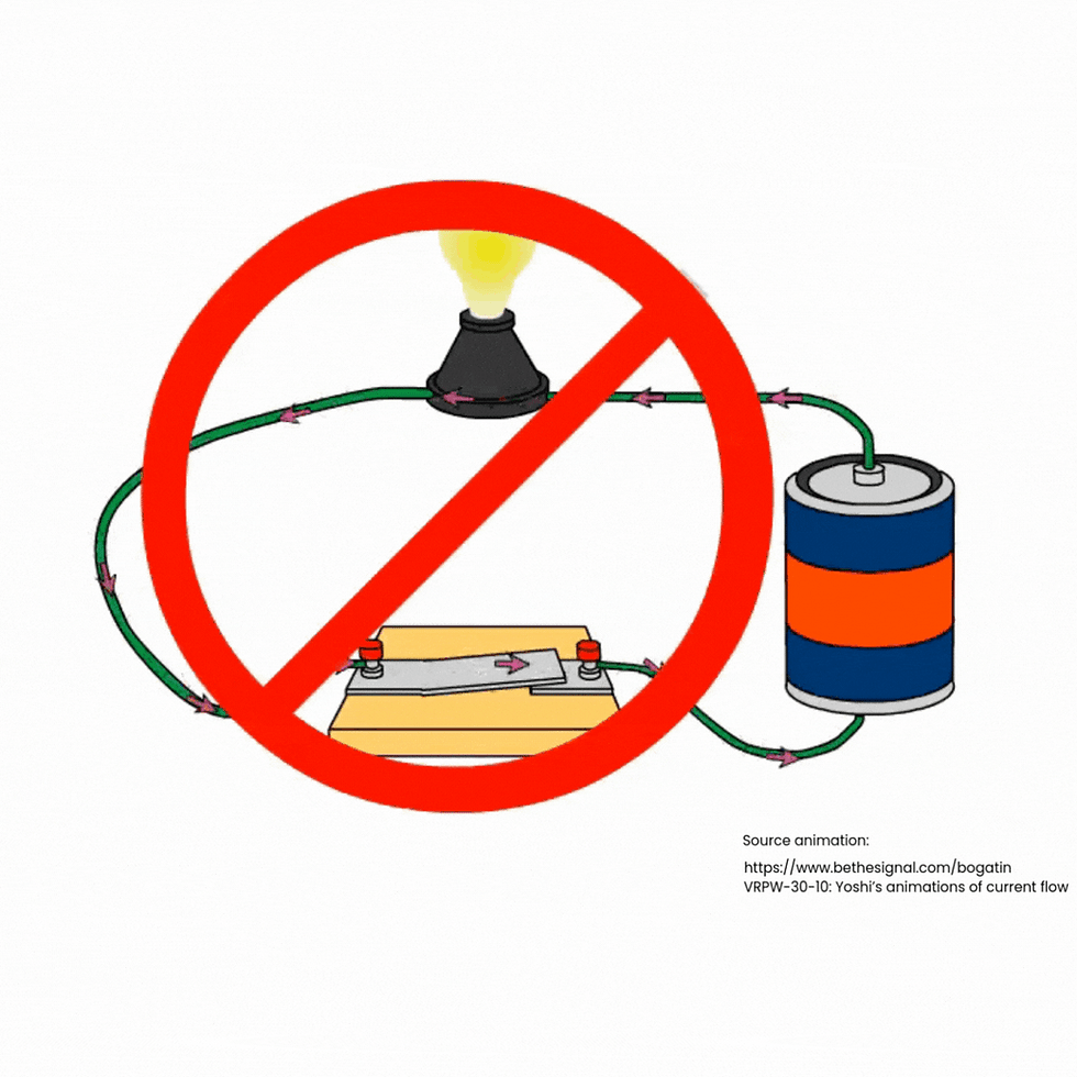
This analogy is helpful for building simple circuits, but does it suffice to describe what really happens inside the PCB?
A more in-depth approach is to think about signal propagation in terms of fields. This requires revisiting the fundamentals: Maxwell's equations.
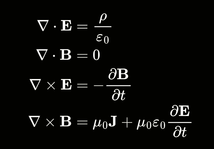
Without delving deeply into the math, the key takeaway here is the fourth of Maxwell's equations: The Ampere-Maxwell law.

This law tells us that a circulating magnetic field (B) is produced by an electric current (J), and by a time-varying electric field (E). Conversely, a circulating magnetic field, generates an electric current, and a time-varying electric field.
These phenomena are represented by two terms:
The electric current density (J)
The displacement current density
the latter, being on the right side of the equation. The first concept, conduction current density, is commonly explained by comparing it to water flowing through pipes. The second concept, displacement current density, can be understood more easily by thinking of the current behavior in a capacitor.
It's often assumed that when a capacitor is charged with a DC signal, no current flows through it.
However, with an AC signal, especially at high frequencies, the capacitor appears to conduct electric current.
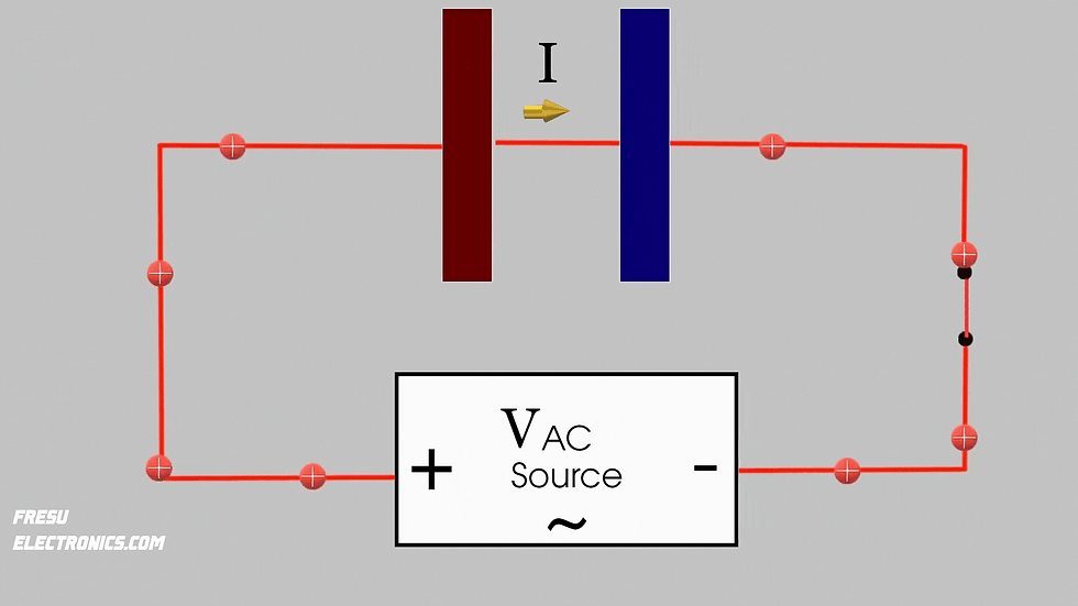
This is not true. In reality, no electric current flows through the plates and dielectric of the capacitor, as this would contradict the definition of a dielectric.
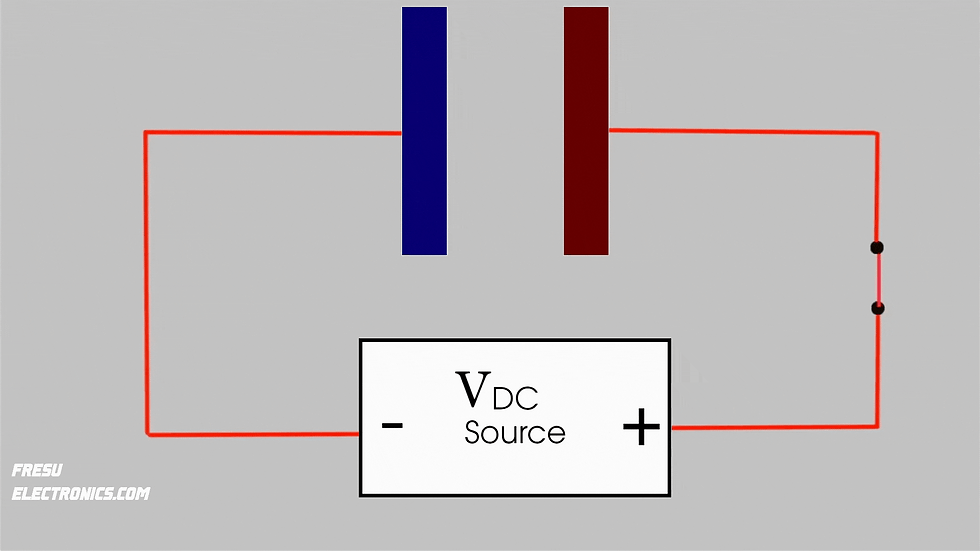
What happens instead, and this is Maxwell's actual contribution to Ampere's law, is that when the capacitor is charging, the voltage change across it, causes a displacement of charges within its dielectric. In the dielectric, bound charges align towards the capacitor's plates.
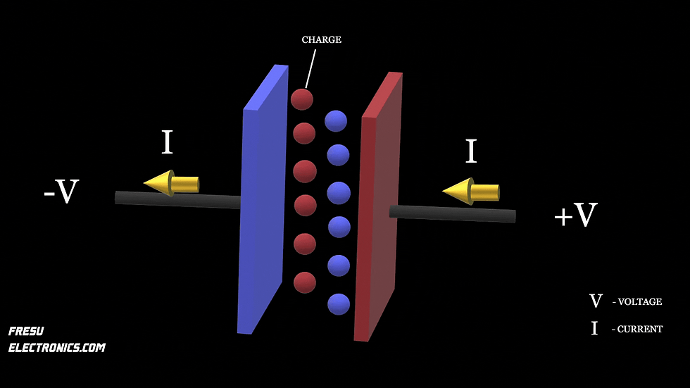
Positive charges on one side, and negative charges on the other.
🔓This movement, which Maxwell called 'displacement,' creates an apparent polarization current through the capacitor known as the displacement current.
Now, considering these concepts of conduction current, and displacement current, how do they connect to PCB design?
Let's consider this model of a PCB, where the metal conductors are shown in yellow on the top and bottom sides. At the top, we have the signal trace connected to the load on the right, and on the bottom side, there's the return plane for the signal, also connected to the load. The green layer beneath the signal trace is the dielectric material, insulating the two metal conductors.

This forms the transmission line for signal transmission. In this model, the two metal conductors separated by a dielectric material can be compared to a capacitor. This comparison helps us grasp what happens when a signal is sent through the transmission line. Moreover, since these are conductors, they naturally have inductance, so to simplify, we can view the PCB as a sequence of small capacitors and inductors.
Now, what happens when a signal is injected into the transmission line?
The propagating signal, at the point where the electric field shifts from low to high, creates a displacement current, forming a current wavefront.
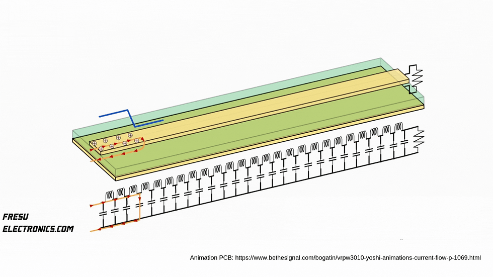
In this situation, we see Maxwell's equations in action.
First, there's the conduction current, which includes the signal current (also called forward current) on the top trace, and the return current on the bottom.
Second, we have the displacement current, which arises from the changing electric field at the front of the signal wave.
🔓 Interesting fact: Until the signal gets to the end of the transmission line, it doesn't 'know' what's at the end!
What happens when the signal reaches the end of the transmission line?
This outcome, is determined by how well the connected load's impedance matches the transmission line's characteristic impedance. If there's a mismatch, meaning the load's impedance is different from the line's, the signal will reflect back.
On the other hand, if the load's impedance perfectly matches the line's impedance, there won't be any signal reflection. This concept is crucial for the entire journey of the signal along the line. At any point where the signal encounters a change in impedance, it can cause a reflection of the signal.
Conclusion
When someone begins their journey in PCB design, the theoretical knowledge gained in classical electrical engineering classes does not always translate seamlessly into practical PCB layout practices. This often leaves hardware designers in a challenging position, learning through trial and error.
At fresuelectronics.com, our primary goal is to help you circumvent the pain associated with this steep learning curve. We believe that by sharing this guide, along with the courses, materials, and programs we offer, we can assist you in navigating the complexities of PCB design.
Our aim is to support you on your path to mastering this field, ensuring that you have the tools and knowledge necessary to succeed.

Comments