

Differential Mode vs. Common Mode Currents
- Dario Fresu

- Nov 18, 2024
- 10 min read
Updated: Feb 24, 2025

Action list:
In this article, we’ll explore the coupling methods of electromagnetic interference (EMI) and delve into the types of currents that EMI generates in printed circuit boards, specifically focusing on differential mode and common mode currents. Understanding these currents is fundamental to designing circuits that can effectively manage interference, maintaining performance across diverse environments.
In one of the previous lessons, we reviewed how electromagnetic compatibility (EMC) breaks down into two main branches: electromagnetic interference, often shortened to EMI, and electromagnetic susceptibility, also known as electromagnetic immunity. These two branches help us categorize and address the different aspects of how electronics interact with electromagnetic energy, whether it’s to prevent unintentional emissions or protect devices from interference. Within these branches, each is further divided for more targeted analysis and control.

For electromagnetic interference, or emissions, we typically separate these into conducted emissions and radiated emissions. For susceptibility or immunity, we similarly split this into conducted susceptibility and radiated susceptibility.
To better understand how these types of emissions and susceptibilities arise and how they travel, it’s important to clarify two main distinctions regarding the origin and distance of a signal. The space around an EMI source divides into two primary regions:
The Near Field region
The Far Field region.
Close to the source, in the near field, we analyze electric and magnetic fields separately. Their properties are influenced strongly by the source itself. As we move farther away, in what’s known as the far field region, these fields merge into what we call an electromagnetic plane wave.

Here, the field characteristics are shaped less by the source and more by the properties of the medium through which they propagate. The boundaries between these regions are determined by the signal’s wavelength.
This separation between near and far fields doesn’t have an exact cutoff point but instead passes through what we call the transition region. Typically, this transitional zone is located at a distance of about lambda over two pi (where lambda represents the signal wavelength), although this can vary.
In the far field, the ratio between the electric field and magnetic field stabilizes, reaching a consistent value referred to as the wave impedance, equal to approximately 377 ohms in free space.
In the near field, however, the ratio between electric and magnetic fields depends on the source and varies with the observation distance. This variability occurs because electric and magnetic fields attenuate differently depending on the type of source.
For example, in a dipole antenna (a source tipically characterized by high voltage and low current), the wave impedance is greater than 377 ohms, making the electric field dominant. Here, the electric field strength decreases inversely with the cube of the distance, while the magnetic field diminishes inversely with the square of the distance. As the distance increases, this ratio lowers until it reaches the wave impedance of 377 ohms.
In contrast, with a source like a loop antenna, where higher current and lower voltage characterize the source, the magnetic field dominates. The electric field, in this case, diminishes inversely with the square of the distance, while the magnetic field weakens inversely with the cube of the distance. This means that in this configuration, the impedance ratio between electric and magnetic fields starts below 377 ohms and rises until it reaches this value.
In the far field, both the electric and magnetic fields attenuate at the same rate, inversely with the distance. Now that we’ve introduced these concepts, we can delve deeper into how noise couples into our circuits.
Coupling Methods
In electronics, several coupling methods influence how noise and signals transfer from one component to another.

These coupling types are broadly classified into four main categories:
Capacitive coupling,
Inductive coupling,
Radiative coupling,
Conductive coupling.
Capacitive coupling
Capacitive coupling occurs when two electrical conductors separated by an insulating material, known as a dielectric, transfer energy between each other through an electric field. This transfer is driven by the capacitance between the two conductors, which allows them to store and release electric charge.

For capacitive coupling to occur, there must be a changing voltage source and two conductors, or metal plates, placed close together. When an electric potential is applied to one of the conductors, it generates an electric field in the surrounding space, which induces an equal but opposite charge on the adjacent conductor.
This induced charge creates an electric potential difference between the conductors. Capacitive coupling often arises unintentionally, especially in circuits with closely spaced conductors or thin insulating layers. This can lead to undesired signal coupling or interference across different circuit sections, or even in neighboring circuits.

While capacitive coupling is deliberately utilized in components like capacitors for energy storage or in touchscreens for detecting inputs, in the realm of EMC, it can lead to signal degradation or interference. As a result, careful design practices are needed to minimize its unintentional effects.
For instance, when two traces run parallel and close together, the changing electric field of one trace can couple into the other via capacitive coupling.
Inductive coupling
Inductive coupling occurs when two conductors transfer energy between each other without a direct physical connection, relying instead on a magnetic field generated by the time-varying current flowing through one conductor. For inductive coupling to be effective, a varying current source and two conductive loops or parallel wires with return paths are needed. These conductors form separate loops that are magnetically linked.

The coupling effect between them can be strengthened by winding the conductors into coils and aligning them on a common axis. Like capacitive coupling, inductive coupling also has practical applications, such as near-field communication (NFC) technologies used in RFID or NFC devices, and in powering medical implants without requiring physical connections. However, in the context of EMC, inductive coupling in the near field requires attention, as it can occur when circuits are closely spaced within a product.
Radiative Coupling
Radiative coupling, on the other hand, involves the transmission of electromagnetic energy between two circuits through electromagnetic waves propagating through space. This type of coupling does not require physical contact and can be intentional, such as in radio communications, or unintentional, where a source circuit emits electromagnetic waves that are then received by a nearby circuit, creating unwanted interference.

Radiative coupling involves two antenna-like structures: one that transmits the interference (the aggressor) and another that receives it (the victim). These can be any conductive components, such as wires, traces, or cables, which may unintentionally radiate or receive signals. Unlike capacitive and inductive coupling, radiative coupling occurs in the far field, typically external to the product.
Conductive Coupling
Finally, we have conductive coupling, where noise transfers directly between circuits through a shared conductor. Here, noise couples into a conductor and transmits through wiring to other circuits, with one common example being interference from a motor coupling into another connected circuit, making it a victim of the noise.

This category also includes what’s known as common impedance coupling. In this case, two circuits share the same impedance path, as seen when both circuit one and circuit two share a common impedance path. The current from circuit one passing through this shared impedance creates a voltage drop in the return path, affecting circuit two by introducing an unwanted voltage in its circuit.
It’s important to recognize that in such scenarios, we must account for not only the resistance of the shared connection but also its inductance. At higher frequencies, the inductive component of this impedance becomes more significant due to its frequency dependency. Therefore, when evaluating the coupling, it’s better to consider the overall impedance rather than focusing solely on its resistive, inductive, or capacitive components individually.
A notable aspect of this phenomenon is its reciprocal nature. If circuit one affects circuit two through this shared impedance, circuit two will similarly impact circuit one, leading to bidirectional interference.
💡 By the way, If you would like to master EMC/EMI design, we have a new training program here:
There, you’ll find details on how to apply for one of our exclusive programs designed to help you achieve that goal.
Differential and Common Mode Currents
Let’s delve into the exciting topic of differential mode currents and common mode currents. This is an area that I initially found quite perplexing until I began to conceptualize these currents in a straightforward manner. Essentially, differential mode currents can be understood as currents flowing in opposite directions, which is precisely why we refer to them as differential or different. On the other hand, common mode currents move in the same direction, and this shared direction is the reason behind the term "common."

If we adopt this perspective, I assure you that it will significantly simplify our understanding of these concepts.
Differential Mode Currents
When we talk about differential currents, the most effective way to visualize them is by considering how signal current flows within a circuit. According to circuit theory, we know that current consistently flows in a loop. This fundamental principle applies here as well, but for clarity’s sake, we will divide this loop into two distinct parts.
We can conceptualize the signal current as being divided into two components:
The forward current,
The return current.
The signal consists of the forward current, which travels from the source to the load, and the return current, which makes its way back from the load to the source. Together, these currents complete the current loop.
🔓 In a previous discussion on signal propagation, I explained that this current loop actually forms instantaneously as the signal moves through the printed circuit boards.
This instantaneous formation is facilitated by what we refer to as displacement current. Thus, this current loop is established even before the signal reaches the load. However, for simplicity in our discussion, we will assume that the signal must first reach the load and then return. Since these currents flow in opposing directions, we can categorize them as differential.

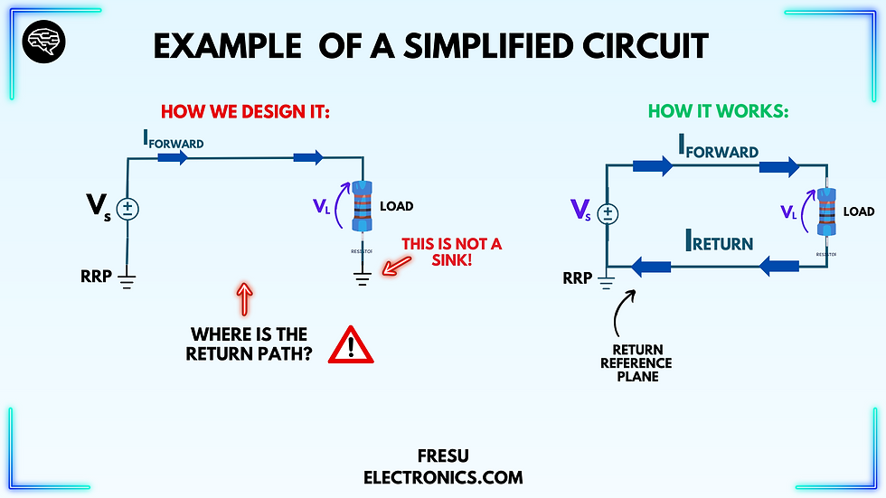
When we have a circuit designed for signal transmission, the differential mode represents the standard propagation mode we have learned about through circuit theory. This is indeed the useful signal. However, it’s essential to remain vigilant about the size of the loop formed by this signal current. As illustrated in the Figure 9, the dimensions of the signal current loop are influenced by both the forward current and the return path.
Consequently, when we are designing these two paths, we must pay careful attention to their distances to ensure that we maintain the loop as compact as possible. Engineering the return path involves not just ensuring that the signal reaches the load efficiently but also guaranteeing that it returns effectively. In the context of printed circuit boards, the loop created by the differential mode current is contained within the PCB itself.
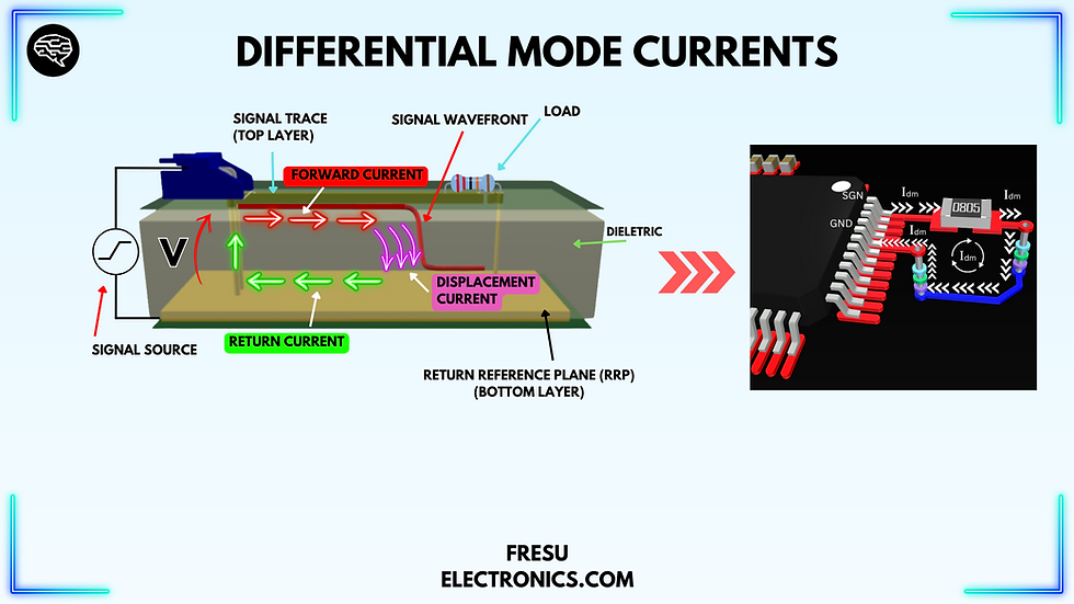
As designers, it is imperative to prioritize this aspect rather than leaving it to chance, as one of the primary considerations is to keep this return path characterized by low impedance. This strategy helps prevent the return current from seeking alternative paths that may have lower impedance back to the source. It is essential to understand that such lower impedance paths can introduce parasitic elements that we are unable to control.
By keeping the forward and return paths closely aligned, we effectively minimize the size of the current loop. Unfortunately, this important consideration is often overlooked because we have adopted simplifications from circuit schematic design, which can inadvertently work against us. For instance, we might mistakenly assume that there is a sink for the currents rather than a proper return path.
A smaller current loop results in lower magnetic fields generated by the currents flowing within this loop, thereby reducing the electromagnetic radiation produced. However, it is also worth noting that a smaller loop is less effective at receiving interference.
One key point to clarify from the Figure 10 is that the circuit is not connected to any external connections, such as earth grounding. This situation changes significantly when we consider common mode currents where the circuit loses its isolation, introducing a parasitic component that creates a larger loop.
Common Mode Currents
We define common mode currents as having a shared characteristic, which is their direction. In this instance, the currents Ic1 and Ic2 run parallel to each other, both moving in the same direction. This configuration implies that the return reference plane not only carries the return current from the signal, as we noted in the differential mode, but also includes the Ic2 current, which represents noise.

This noise current flows in the opposite direction to the return current we observed previously.
🔓 It is important to emphasize that these two currents are not part of the original signal and can be categorized purely as noise.
Thus, the common mode current consists of the forward Ic1 and also the forward Ic2, forming a loop closed by the return current Ic through the earth ground parasitic elements indicated.
These parasitic elements can vary considerably; for instance, they may include capacitance between the cables connected to the circuits and the earth ground or the inductance associated with the system chassis and its connection to earth ground via the thin cables we utilize.
The challenge presented by the common mode current loop is that it is often larger and, importantly, uncontrollable. This contrasts with the differential mode current loop, which remains confined within the circuit and is carefully designed by the printed circuit board designer. Interestingly, even a minute common mode current in the microamp range can lead to electromagnetic compatibility (EMC) failures and significant emissions.
Moreover, since common mode loops are generally larger than differential mode loops, their capacity for radiation is notably higher. This characteristic also implies that, regarding immunity or susceptibility, even minor interference can be effectively captured by this loop and potentially disrupt the entire system.
One significant distinction between the signal current in differential mode and the interference in common mode lies in the propagation dynamics. The signal in differential mode cannot propagate without a designated return path, while common mode currents and their accompanying interferences will invariably find their own return path, typically through parasitic elements that were either unaccounted for or not designed into the circuit.
It is essential to remain cognizant of several factors, particularly when working with differential pair connections. In these scenarios, maintaining symmetry between the two conductors is vital to avoid any conversion from differential mode propagation to common mode propagation. Failing to do so can lead to the creation of common mode currents that may result in interference issues, ultimately causing significant disruptions in the electronic circuits we have designed.
As we explore the exciting world of EMI, you might be wondering how you can deepen your knowledge and skills in this area. If you would like to master EMC/EMI design, we have a new training program here:
There, you’ll find details on how to apply for one of our exclusive programs designed to help you achieve that goal.


Comments