

Understanding ESD: How to Protect Your Electronics from Electrostatic Discharge
- Dario Fresu

- Nov 18, 2024
- 28 min read
Updated: Apr 23, 2025

In this lesson, we will discuss electrostatic discharge, or also known as ESD, and explore how to mitigate the EMI issues this phenomenon creates in our electronic products and printed circuit boards.
Understanding Static Electricity in Circuit Board Design
One of the significant phenomena we must consider when designing printed circuit boards is the occurrence of static electricity. Specifically, we need to focus on the discharge event commonly referred to as electrostatic discharge (ESD). ESD can be viewed as a particular case of immunity to transient interferences.
To fully grasp this phenomenon and its implications, we first need to examine how static electricity is generated. Static electricity forms when two objects accumulate an electric charge through processes such as induction or friction. This can happen, for instance, when two materials come into contact and rub against each other, resulting in the transfer of electrons between them. The underlying cause of this transfer lies in the differences in energy levels between the two materials.
When a charged material interacts with another, it can either attract or repel the electrons of the second material, leading to the creation of an induced charge. As a result, a positively charged area is produced in the second material, which in turn causes an attraction between the two.

There are various methods through which static electricity can be generated. Some common examples include the triboelectric effect, the piezoelectric effect, and induction charging, among others. Focusing on the triboelectric effect, this phenomenon occurs when two materials with differing electrical properties are rubbed together, leading to the generation of electrostatic charges.
But what do we mean by "electrical properties"?
These properties are outlined in what is known as the triboelectric series. This series ranks materials based on their tendency to either give up electrons or acquire them. Essentially, the triboelectric series serves as a guide to help us understand how different materials interact with one another in terms of charge transfer.

The materials at the top of the triboelectric series will tend to transfer charge to those at the bottom. However, it’s important to note that just because a material is ranked higher doesn’t necessarily mean it will create a greater amount of charge transfer. The actual transfer of charge is influenced by various factors, including the smoothness of the surfaces in contact and the speed at which the two materials are separated.
For us to effectively understand the ESD phenomenon, we must recognize that many issues arise from materials with low charge mobility. This low mobility allows charges to accumulate on the surface of the materials, leading to a higher potential difference. For instance, if we take two conductors with high charge mobility and separate them, we won't observe any triboelectric charging. In this case, as soon as we begin to separate the materials, the charges will not accumulate but will return to their original state.Thus, our focus should shift to situations where an insulator comes into contact with a conductor.
We previously mentioned that static electricity arises from low charge mobility in materials, which means that the charges primarily exist at the material's surface rather than throughout its interior. In insulators, this localized charge does not disperse through the material; instead, it remains concentrated where it was generated. This behavior contrasts sharply with conductors, where charges can move freely across the surface. Consequently, when we ground an insulator, nothing occurs because the charges cannot migrate from their initial location. In contrast, grounding a conductor will effectively remove excess charges.
🔓 A key point to remember is that the charge typically originates in the insulator, where it remains stationary, and can then be transferred to a conductor either through direct contact or induction.
Once the charge is present in the conductor, where it is free to move, the risk of electrostatic discharge increases, especially if this conductor is brought near another metallic object. In such cases, the potential for ESD becomes a significant consideration in circuit board design, and understanding these interactions is essential for preventing issues related to static electricity.
This process can happen even when the metallic object in question is not directly connected to an earth ground. The current can still flow through the parasitic capacitance that exists between the metal and the earth ground. This mechanism is essentially how transient events occur, operating on principles similar to those found in alternating current (AC) systems within a capacitor.
During an ESD event, the current does not travel through the protective earth connection, which is often represented by the green and yellow wire. This wire presents a high impedance to the ESD discharge. Instead, the ESD charge flows through the parasitic capacitance formed between the metallic object and the earth ground, effectively acting like a capacitor.

This explains why we can sometimes feel an ESD event, for example, when we touch a door handle that is not directly connected to earth ground. The sensation arises due to the capacitance between the door handle and the earth ground.
When we consider a charged element, whether it is an insulator or a conductor, it will create a static electric field around it due to the presence of these charges. If this charged object is brought near another neutral conductor, it induces polarization or displacement of charges within the neutral conductor. This means that the charges in the neutral conductor will begin to align in a specific direction to counterbalance the applied charge from the charged object, effectively creating its own electrostatic field.
If the electrostatic field source is negatively charged, the side of the neutral conductor closest to it will become positively charged, while the opposite side will acquire a negative charge. Importantly, this process does not alter the overall amount of charge contained within the neutral conductor; instead, it changes how this charge is distributed across the conductor's surface.

If we remove the charged object, the charges in the neutral conductor will redistribute, allowing the conductor to revert to a neutral state. However, if the source of the electrostatic field remains close, the charges will continue to remain separated, with positive charges accumulating on one side and negative charges on the other.
Now, if we connect this polarized conductor to earth ground, this connection allows the excess charges on the negatively charged side of the conductor to flow into the ground, effectively neutralizing that side of the conductor. The charges will seek a balanced state between the external charge from the electrostatic field source and the charges present in the conductor.
Should we suddenly remove this ground connection while the source of the electrostatic field remains nearby, the conductor will retain a charge. The charges that flowed to the earth ground will be lost, leaving the conductor charged with the remaining charges.

This scenario illustrates how charges bound in an insulator can influence the movement of charges in a nearby conductor, ultimately resulting in the creation of additional charged objects.
In the table below, we can observe how certain common daily activities can generate significant electrostatic voltages. Additionally, it highlights how these voltages are highly influenced by the humidity level in the surrounding air.

Being aware of this relationship allows us to leverage it for our benefit and helps us understand the environmental implications on our devices and their users regarding how ESD can affect circuit performance.
Attraction of charges
We previously noted that charges in a conductor spread across its surface when subjected to an external charge. But why does this occur?
The answer lies in the attraction between opposite charges and the repulsion between like charges. This interaction causes charges to redistribute, effectively moving apart from each other.

However, this movement is confined to the surface of the object; once the charges reach the surface, they cease to move inward. This indicates that no accumulation of charges will occur within the conductor itself.
The intriguing part arises when we provide a pathway for the surface charges to flow. Given that the mobility of charges within a conductor is high, these surface charges can easily move away. A common example of this is when we connect a conductor to an earth ground.
So does this mean conductors are inherently more dangerous than insulators, leading us to disregard the risks associated with insulators when discussing ESD?
Not quite. The potential danger of an insulator lies not in the charges it contains, but rather in its ability to induce a charge in a nearby conductor. This induced charge can lead to the occurrence of an electrostatic discharge event.
Everything begins with these charges and the electrostatic fields that surround them. Understanding this is crucial, as it lays the groundwork for the concept of free space capacitance, which I will explain next.
Free Space Capacitance
Now, let’s delve into how free space capacitance differs from the more traditional concept of parallel plate capacitance that many of us are already familiar with. Free space capacitance can be conceptualized as the capacitance of an object relative to the space surrounding it. To calculate this, we start by comparing the surface area of the object to the surface area of a hypothetical sphere.

To calculate the free space capacitance of an object, we first determine its surface area and then create a sphere with the same surface area. The free space capacitance is the capacitance between this sphere and another sphere with an infinite radius that surrounds it. We use a specific formula, derived from the capacitance formula for spheres, to find this value.
🔓 A key point to grasp is that every object has an associated free space capacitance.
The formula provided in Figure 8 can be used to calculate this capacitance in picofarads, where 𝑅 represents the radius of the sphere that shares the same surface area as the object being measured.
As a reference, we can approximate that the typical capacitance of a human is around 50 picofarads. Of course, this is just an approximation to illustrate a point. For comparison, the Earth has an approximate capacitance of about 700 microfarads.
Capacitance between parallel plates
In addition to free space capacitance, we also need to account for the capacitance between two metal plates, which is essential for understanding how discharge events can occur between objects that are not physically connected.

The formula to calculate this capacitance is derived from classical physics, where:
𝜖 is the dielectric constant of the medium between the plates,
𝐴 is the area of the plates,
𝐷 is the distance separating the plates.
Both the formulas for free space capacitance and parallel plate capacitance are integral in determining the total capacitance of an object.
Now that we have established this foundational concept, we can apply it to calculate the total capacitance of a person, allowing us to model the electrostatic discharge effects that users can exert on our devices. This understanding is essential because humans can accumulate electrical charges, and due to our conductive nature, we have the potential to transfer these charges during an electrostatic discharge event to sensitive equipment or electronic circuits, leading to possible damage.
Human Body Model
In modeling the human body for ESD effects, we typically consider the equivalent area of a human as a sphere with a diameter of one meter. This approximation gives us a free space capacitance of approximately 50 picofarads, as previously mentioned. However, in addition to this free space capacitance, we must also account for the parallel plate capacitance. This means we need to evaluate how the capacitance of our body is influenced by our surrounding environment.
💡 By the way, If you would like to master EMC/EMI design, we have a new training program here:
There, you’ll find details on how to apply for one of our exclusive programs designed to help you achieve that goal.
For instance, consider the soles of our feet in contact with the earth ground and our hands, or fingers touching walls, or other structures. There will be a certain amount of parallel capacitance between these various elements, and it’s important to include all these variables when calculating the overall model of our body.

The total equivalent capacitance typically used for this human body model ranges from about 50 picofarads to 250 picofarads. Once we establish this total capacitance, we must also consider the electrical resistance of the body. This aspect is significant because as our bodies accumulate charge, a voltage potential builds up, and resistance plays a critical role in determining how the current flows through us and eventually discharges onto another object. Notably, the resistance can vary based on contact points; for example, the resistance of our fingertip differs from that of the palm of our hand.
The typical resistance of the human body is generally measured between 500 ohms to 10 kilo ohms. However, if we are in contact with another conductive material, such as holding keys, this resistance can drop as low as 50 ohms. Thus, incorporating resistance into the human body model is essential for simulating scenarios where users touch a device or merely approach it. This understanding allows us to establish testing procedures to evaluate our devices against these ESD phenomena effectively.
Testing
With an equivalent model in place, we can create instruments for testing. A typical, straightforward electrical model used during such tests is the ESD gun, which consists of a discharge capacitor and an equivalent series resistance. The component values can vary based on specific standards, but common values, such as those specified in the EN 61000-4-2 standard, are around 150 picofarads and 330 ohms.
Let’s examine the waveform of the ESD discharge applied during standard ESD tests. The ESD discharge waveform comprises two distinct waveforms.

The first waveform exhibits a sharp rise time attributed to the free space capacitance of the probe's tip, while the second, slower waveform results from the 150 picofarad capacitance in series with the tester's ground strap inductance.
Typically, the ESD waveform features a rise time ranging from 0.7 nanoseconds to 1 nanosecond, although these parameters may vary based on the applicable testing standards, which should be referenced accordingly. The discharge voltage can vary, typically ranging between 4 kV with a current of 15 A and 8 kV with a current of 30 A.
🔓 It's worth noting that some devices are already sensitive to discharges of only a few hundred volts.
The challenge arises when the discharge voltage is low, as we often cannot sense it, making debugging ESD failures particularly difficult. In contrast, when we encounter electrostatic discharges with voltages exceeding 20 kV, the effects are readily noticeable, often resulting in painful experiences.
Discharge through the door handle
Now that we have established a foundation for understanding electrostatic discharge (ESD) events, let’s examine one of the most common scenarios we often encounter: the ESD discharge that occurs when we touch a door handle. This example is helpful for illustrating the underlying principles at work during such events.

The soles of our shoes are typically made of insulating materials, which can become charged through contact with carpets or other materials. This phenomenon relates to the triboelectric effect, where certain materials gain or lose electrons upon contact. As a result, the charge builds up on the insulative soles of our shoes.
Although these charges are trapped in the shoes and cannot move freely due to their insulating properties, they can still influence the charges in our bodies, which are conductive. When we approach a conductive object, like a door handle, the accumulated charges on our body tend to redistribute themselves, causing an accumulation of charge at the extremities of our skin. If we touch the door handle, grounding that point, for instance at the tip of our finger, the charges can discharge, resulting in an ESD event.
The intriguing part of this phenomenon is that the door handle, while a conductor, does not need to be directly wired to an earth ground for the discharge to occur. This happens because of the parasitic capacitance between the door handle and the earth ground. Since ESD is a transient event, the charge will find this capacitance and behave as if it is a short circuit. Thus, the door handle effectively appears to be connected to ground, allowing the ESD event to take place. This situation is analogous to a capacitor connected to an alternating current (AC) source.
Migration of charges
Next, let’s discuss how charges can leave a charged body or object. There are two primary mechanisms: arcing and leakage. Leakage can occur in a few ways, not just through direct contact with a conductor. For example, when touching the door handle, the amount of humidity in the air also plays a significant role. Higher humidity increases the number of water vapor molecules in the air, which serves as charge carriers, making the air more conductive and facilitating charge recombination.

Another method of charge leakage occurs when a charged conductor is grounded. This principle is particularly important in electronic labs, where ESD wrist straps connect to grounding systems to allow for the safe leakage of charges from the body, acting as a conductor, to the ground.
However, this connection is still limited by the resistance of the bracelet. A direct connection without any resistance could pose dangers, particularly if a fault occurs in the grounding system. Thus, the bracelet not only aids in the discharge of accumulated charges but also limits the discharge current, which could otherwise be excessively high.
In addition to the charges escaping conductors, we must also be aware of the issues created by the electromagnetic fields generated by ESD events. These fields can disrupt circuits even when they are located at a distance from the site of the ESD event and are not physically connected. This is possible because the sharp and rapid rise time of the discharge event generates electromagnetic fields with sufficient energy to affect sensitive electronic devices.

These electromagnetic fields become especially problematic in the case of plastic enclosures, which offer little to no shielding against such fields. Therefore, it is essential to consider both the direct effects of ESD events and the potential impact of the electromagnetic fields they produce when evaluating device vulnerability.
Methods of ESD protections
Now that we have a grasp on how ESD can affect devices, let’s delve into the methods we can implement to protect our circuits from such disturbances.
These methods generally fall into several categories:
we can limit or avoid charge buildup,
insulate devices,
provide alternative discharge paths,
shield devices from electromagnetic fields,
and reduce the loop area to minimize the effects of magnetic fields.
The more we can integrate these protective measures into our design, the better we can safeguard our devices against the disturbances caused by ESD events.
Before we discuss these methods in detail, let’s briefly touch on the types of disturbances we aim to prevent.
ESD can lead to various issues classified by their disturbance level:
Hard Errors: These occur when a device is physically damaged, meaning it cannot function properly until a component is repaired or replaced. An example would be an integrated circuit (IC) that burns out due to a discharge.
Soft Errors: These are cases where no physical damage occurs, but the device's operation is disrupted. For instance, a device may freeze or reset unexpectedly without any visible damage.
Transient Upsets: This category describes disruptions in device operation that are temporary. The device resumes normal functionality after the ESD event has concluded.
Transient upsets are particularly relevant, as they fall under Criterion B of the EMC directive, which states that products should withstand at least transient upsets without permanent damage.
ESD Protection strategies
One of the primary strategies for protecting sensitive circuits from ESD events is to ensure that the discharge does not reach these circuits.
Here are several approaches:
Insulation: One way to prevent ESD from affecting the circuit is through complete insulation of the device. This means ensuring that all parts of the device are insulated so that no sparks can occur across any gaps. This method is especially important for components like keyboards or touch panels.
Alternative Discharge Paths: If complete insulation isn’t feasible, providing an alternative path for the discharge current can effectively divert ESD away from sensitive circuits. A common practice is to use a metallic enclosure to direct the discharge.
🔓 When using a metallic chassis, all metallic components must be bonded together with low impedance connections.
Electrical discontinuities, such as gaps that create high impedance paths, can allow the discharge to find alternate routes and potentially reach sensitive circuits, leading to damage. The goal is to create a low impedance path for the ESD current to follow while ensuring high impedance points where we want to prevent the current from flowing.
It’s important to note that we refer to impedance rather than just resistance because impedance accounts for the effects of frequency. ESD events can have rise times in the nanosecond range, so a connection to the earth ground alone might not provide sufficient protection. The earth ground cable, typically colored yellow and green, can present a high impedance path for ESD.

Interestingly, the preferred path for an ESD event often follows the parasitic capacitance between the device under test and the earth ground. Our task, therefore, is to maximize this parasitic capacitance to minimize impedance. By doing so, we encourage the ESD event to follow this path rather than passing through sensitive circuits.
Understanding ESD Events and Their Impact on Circuit Design
Now, practically speaking, we need to consider how electrostatic discharge (ESD) events can reach our devices and subsequently enter our circuits. The main entry points for ESD discharges in a device typically include cables, the enclosure, and points of direct contact with users.
For instance, consider components such as LCD displays, keyboards, touchpads, and other interfaces. Each of these entry points represents a potential vulnerability for our devices concerning ESD. These points must be regarded as significant bottlenecks when evaluating ESD risks in our designs.
This brings us to a very important consideration:
🔓ESD prevention should not be an afterthought left until the final stages of the design process.
Instead, it is essential to integrate ESD considerations at the earliest possible stage of development. The sooner we address these issues, the better our devices will be able to withstand ESD events.
To simplify the process, we can categorize ESD prevention into three main stages:
The first stage focuses on preventing or minimizing ESD events from reaching our circuit.
The second stage involves enhancing the robustness of sensitive circuits, ensuring they can handle ESD interferences should they occur.
Finally, in stage three, we must ensure that the software is fortified to detect and recover from ESD events.
As we delve deeper, let’s explore each of these stages in more detail.
First stage:
In the first stage, where our primary goal is to prevent ESD from reaching our circuit, we can break this down into three key parts:
Firstly, we need to ensure that the enclosure of the device is designed with ESD protection in mind. This means selecting materials and structures that can effectively shield sensitive components.
Secondly, we must apply shielding to the cables. It’s important to confirm that these shields are properly terminated to avoid high-impedance connections with the chassis or circuit board. We should also avoid creating pig-tail connections that could compromise our ESD protection.
The third point in this stage involves ensuring that all external conductors are adequately equipped with transient protective devices. This includes managing unshielded cables that may be at risk of ESD events, thereby preventing any discharge from reaching the internal circuit.
Second stage:
Moving on to the second stage, it becomes vital to ensure that the internal circuits are robust enough to withstand potential ESD events. This includes verifying that all sensitive signal traces are equipped with either filtering mechanisms or protective components that can effectively manage ESD occurrences. Examples of sensitive traces include interrupt lines, reset lines, and other critical inputs that have control functions, whether for our device or for external systems.
Third stage:
Now let’s discuss the third stage, where we focus on strengthening the software aspect of our design. While this may not be a primary concern for hardware designers, it still requires a collaborative effort to implement correctly. It’s essential to keep all team members informed about these stages and to support one another throughout the process.
During this phase, our objective is to ensure that any faults can be detected accurately. It’s also important that the measurements taken are precise so that the software can effectively recognize these issues and respond accordingly. Common problems can arise, particularly when ESD events lead to memory corruption. I recommend that software development closely tracks the hardware development, as both teams can benefit significantly from this partnership. Thus, a solid collaboration between software and hardware designers is necessary for effective ESD management.
Product Enclosure
One major consideration during the project development process is the type of enclosure we choose for our device. Generally, we can categorize enclosures into two main types: metallic and non-metallic.
The advantage of a metallic enclosure lies in its ability to act as a conductor, helping to divert ESD events away from sensitive circuitry. However, there is a downside. While metallic enclosures can help manage ESD, they also facilitate the occurrence of ESD events, similar to any other conductive material.
A common misconception that we have already addressed is that the ESD event uses the earth-to-ground conductor connected to the chassis as its primary discharge path. However, this is not entirely accurate, as the earth-to-ground connection typically presents high impedance during the transient response of an ESD event.
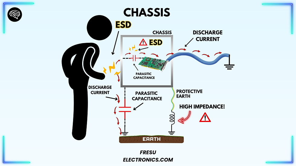
What truly aids in ESD management is the parasitic capacitance between the chassis and the earth ground. As previously described, this capacitance provides the path through which the majority of the ESD current will flow. Thus, when we consider optimizing the ESD path, we must focus on minimizing impedance, which can be achieved by enhancing the parasitic capacitance between the chassis and the earth ground.
Let’s delve into what occurs when an ESD event takes place and how we should establish connections to protect our circuits. In the first scenario, we have a user who, after walking on a carpeted floor, approaches the chassis of the device. This individual now carries a charge that can initiate an ESD event upon contact with the device's chassis. When this discharge occurs, the current flows through the chassis and uses the parasitic capacitance path to discharge into the earth ground.
A question arises: what happens to the electronic circuit located inside the chassis?
If the product is fully isolated from its surroundings, meaning the chassis has no openings and effectively contains the internal devices without seams or external cables, the electronic components within the chassis will experience a rise in voltage that matches the ESD discharge. This phenomenon occurs because there is still some capacitance between the electronic circuits and the chassis.
Under these conditions, the circuit is not put at risk because the reference voltage within the circuit will increase to the same level as the chassis voltage. Consequently, there won’t be a difference in potential between the two.
However, complications arise when the chassis is not completely isolated. If there are cables extending from the chassis that connect to other reference voltages outside our system, this can create significant issues.

Why does this present a problem?
When the ESD event occurs, the chassis voltage will increase, but the internal circuit remains at the same voltage level as the external cable reference. Here, we’re discussing situations where the circuit does not have a direct connection to the chassis itself. In this case, the chassis can attain a substantially higher voltage compared to the circuit within. This creates the potential for a secondary ESD discharge to occur between the chassis and the internal circuit.
The primary concern with this secondary discharge event is that, unlike the initial spark, which was limited by the user’s resistance, there is no resistance to moderate the discharge between the chassis and the internal circuit. The only limiting factor is the parasitic capacitance between the chassis and the printed circuit board (PCB). This absence of resistance means that this discharge event can be significantly more severe and pose a greater threat to the circuit.
In quantifiable terms, we may be dealing with a discharge current of around 100 amps, as opposed to the 10 amps we previously encountered when the user’s resistance limited the current. Therefore, it is essential to be cautious in scenarios where the PCB is not connected to the chassis. We should aim to increase the distance between the chassis and the PCB, ensuring that the impedance between them is sufficient to withstand the voltages dictated by relevant standards.
💡 By the way, If you would like to master EMC/EMI design, we have a new training program here:
There, you’ll find details on how to apply for one of our exclusive programs designed to help you achieve that goal.
This issue is also related to how the chassis is connected to the earth ground system. If the chassis is grounded, the voltage will not rise as sharply because this connection will allow some of the discharge current to flow through it, effectively lowering the chassis voltage. On the other hand, if there is no connection to earth ground, the chassis can quickly reach the full potential of the ESD event, which poses a much higher risk to our circuit.
To protect the circuit when no connection to the chassis is present, it is imperative that the distance between the PCB and the chassis accounts for the higher voltage levels that the chassis can achieve during an ESD event. According to Henry Ott's recommendations, we should ensure a voltage separation of at least 2 kV when the chassis is connected to earth ground and a minimum of 15 kV when it is not grounded. These recommendations apply particularly to cases where the chassis cannot be directly connected to the PCB.
If direct connection is possible, the best approach is to link the PCB reference plane to the chassis at a single low-impedance point. The rationale behind using a single low-impedance connection is that it allows the reference plane to rise to the same voltage level as the chassis. This ensures that there is no discharge occurring between the chassis and the PCB. Moreover, we want to avoid ESD currents traveling through the PCB when connected at multiple points.

For optimal protection, we should connect the PCB to the chassis at a single, large impedance point, ideally situated close to the input and output connectors of the board. It’s critical to emphasize that this connection should maintain low impedance. A small impedance could facilitate the generation of common mode currents, which can lead to issues concerning radiated emissions. Therefore, while we’re advocating for a single connection point, it must be a low-impedance connection—not a pigtail, but rather a robust connection.
In situations where it is not feasible to connect the PCB reference plane to the chassis directly, we can consider employing a secondary metallic plate. This plate should connect to the reference voltage of the PCB, effectively acting as a barrier that blocks capacitive coupling between the PCB and the chassis. Essentially, this plate serves as an alternative chassis.

Another important consideration arises when two systems are interconnected with cables. If one PCB has a single low-impedance connection to the chassis, it may function correctly. However, if that circuit lacks additional protections, the ESD can propagate through the cables, initiating a sequence of further discharges. It’s vital to be aware of these interconnections and ensure that all connected systems have adequate ESD protection.
Regarding cables, they present unique challenges as they serve as direct entry points for electrostatic discharge into the device. Additionally, cables can act as potential antennas, capable of picking up electromagnetic fields generated by ESD events occurring at a distance from the device. This can lead to unintended consequences, especially when the cables connecting the systems become receivers or transmitters of electrostatic discharge.
Addressing Issues with Cables and ESD Protection Strategies
Now, let’s examine the challenges posed by cables and explore various strategies to prevent electrostatic discharge (ESD) events from reaching our circuits.
We have several options available for cable management and ESD protection. One effective method involves using shielded cables. In this approach, the shield acts as an extension of the Faraday cage, protecting the cables from external ESD influences. Another option is the implementation of transient voltage suppression (TVS) devices. These components can effectively divert electrostatic discharge away from sensitive circuits. Additionally, we can utilize common mode chokes, which increase the impedance perceived by an ESD event. Bypass filters are also a viable solution to mitigate ESD impacts. Each of these methods offers varying levels of protection for the system.
Shielding:
Using shielded cables helps maintain the integrity of the Faraday cage that the chassis provides. It is crucial to avoid compromising this protective barrier, particularly at the connection point between the shield and the chassis. This connection should be a 360-degree low-impedance interface. By ensuring this connection is solid, we can provide a direct discharge path for ESD currents to travel, allowing them to reach the chassis and subsequently dissipate through the parasitic capacitance into the earth ground.

TVS devices:
Moving on to transient voltage suppression devices, these represent one of the most effective strategies for managing ESD events. TVS devices allow us to redirect the ESD path strategically, which is why it's vital to understand where to connect them. Ideally, TVS diodes should be placed between the cable we wish to protect and the chassis of the device, rather than connecting them directly to the PCB "ground". This configuration enables us to divert the ESD before it reaches the circuit, facilitating its propagation through the chassis to safely discharge into the earth ground without damaging the internal components.

Filters:
The same principle applies when using filters. It’s best to connect filters from the cables they are designed to protect directly to the chassis. As with TVS diodes, this connection must also be low impedance to ensure it becomes the preferred path for electrostatic discharge. However, one limitation of filtering is that it can only mitigate the impact of ESD on the device; some portion of the discharge may still pass through.

Given this limitation, ensuring robust protection from a software perspective is essential. Typical filters, such as low-pass filters, consist of a resistor that limits the discharge current and a capacitor that filters out the high-energy components of the ESD pulse.
Common-mode chokes:
Common mode chokes serve a similar function, dissipating most of the ESD energy across the choke. Regardless of the method chosen, it is vital to position these protective devices as close to the cable inputs as possible. They should not be placed in the middle of the circuit board or near microcontrollers and processors.

If the PCB is connected to the chassis, the protective devices should be positioned near the point of connection with the cables to maximize their effectiveness. A common pitfall occurs when protection is applied on one side of the PCB while the chassis connection is made on the opposite side. This configuration can create a significant risk for the circuit. In such a scenario, ESD interference can traverse the entire PCB, bypassing the protection, and discharging into the chassis before returning to earth ground.

Therefore, strategic placement of ESD protection devices is paramount for safeguarding the internal circuitry from potentially damaging ESD events.
ESD Protection in Plastic Enclosures
Now that we've discussed the challenges associated with metallic enclosures, let’s explore what happens when we have plastic enclosures. One significant advantage of plastic enclosures is that they do not trigger ESD events as metal chassis do. However, they present their own set of challenges, particularly regarding ESD protection.

Plastic enclosures often have openings that do not fully insulate the internal components from ESD events. Consequently, electrostatic discharges can still reach the circuit and potentially cause damage. Moreover, plastic does not provide protection against electromagnetic fields generated by ESD events occurring nearby. Additionally, the absence of a metallic chassis means there is no alternative discharge path for ESD.
In this situation, relying on protective earth wires is insufficient, as they typically offer high impedance connections. Therefore, we need to explore alternative solutions for mitigating ESD disturbances when a plastic enclosure is in use.
Here, I’ll rank the available options from best to least effective.
Using an Extra Metal Plate:
The most effective approach is to incorporate an additional metal plate to create an alternative ESD path. This metal plate can enhance the parasitic capacitance between itself and the earth ground, facilitating the discharge of electrostatic energy. It is crucial that this plate is larger than the PCB to maximize capacitance and minimize impedance.

All protective measures—such as TVS devices, filters, and shields—should be connected with low impedance to this metal plate instead of directly to the PCB. This ensures that the ESD current is diverted to the metal plate rather than passing through the sensitive circuit.
Connecting to the Return Reference Plane:
If a metal plate is not feasible, the next best option is to connect the cables and shields to a designated portion of the return reference plane on the circuit board.

This method helps limit ESD current flowing through the PCB but does not completely eliminate the risk of ESD affecting the circuit. In this case, it is vital to ensure that the software is robust enough to handle disturbances caused by ESD events.
Direct Connection to the PCB:
If neither of the previous options is available, the final approach is to connect all filters, TVS protections, and shields directly to the return reference plane of the PCB.

Unfortunately, this method provides the least amount of protection, as ESD currents can traverse the entire PCB, using its capacitance to discharge into the earth ground. This situation is likely to create noise and disturbances that could impact the circuit adversely.
When using plastic enclosures, it is essential to pay close attention to the PCB's positioning within the enclosure. Keeping the PCB away from any apertures is critical, as these are potential entry points for electrostatic discharge. Furthermore, there is a heightened risk that electromagnetic fields generated by ESD events can couple with the circuit, leading to interference.

Given that we cannot fully prevent ESD from reaching the circuit, we must focus on fortifying the internal circuitry to withstand any remaining noise or interference. This process will involve making necessary adjustments, and improvements during the development phase to ensure that the device can function reliably, even in the presence of ESD events.
To enhance the robustness of sensitive circuits, especially for components like reset lines, control signals, and interrupts, it’s critical to implement effective filtering techniques. For example, using bypass filters on reset lines can prevent unwanted interference from inadvertently triggering a reset. It’s vital to ensure that any filtering methods employed are suitable for the specific application, considering factors like capacitance limitations of certain interfaces.
Understanding Grounding in ESD Protection
One point of confusion in ESD protection is the concept of "ground." This term can refer to multiple grounding points within a system, leading to potential misunderstandings.

Ideally, we want ESD discharges to be directed to the earth ground. However, as previously mentioned, relying solely on earth ground cables is not feasible since they tend to have high impedance, which hampers ESD discharge effectiveness.
To mitigate this issue, we should focus on enhancing the free space capacitance of the device and the enclosure. By increasing this capacitance, we can lower the impedance of the device to the earth ground, enabling the displacement current from ESD events to discharge more effectively.
When protective measures such as filters, TVS diodes, and shields are employed, they should be connected to the chassis or metal plate (in the case of plastic enclosures) to ensure that ESD energy is diverted properly to the earth ground. If neither a chassis nor a metal plane is available, our best option is to limit the potential ESD damage to the circuit.
However, the level of protection in this scenario will not match that of complete diversion, emphasizing the need for robust software to maintain operational integrity and meet EMC testing criteria.
To illustrate the concept of free space capacitance, consider a smartphone. Although it lacks a direct ground connection, it can still experience ESD discharges.

To mitigate this, we can increase its free space capacitance by adding metal plates or foils, which help redirect ESD safely to the ground.
Coupling Mechanisms of ESD Events
ESD can couple with devices in various ways, primarily through direct contact or via electromagnetic fields produced by discharges. Consequently, we must be mindful of both the enclosure and the layout of the circuitry, which can act like antenna paths for these events. There are two main coupling types to consider:
Inductive Coupling: This occurs when the magnetic field generated by an ESD event interacts with an antenna-like loop structure in the layout or cables. It’s essential to minimize the loop area, as a larger area can make the layout a more effective receiver or transmitter of magnetic fields.
The voltage induced by a discharge current is described by the following equation:

where:
𝐴 is the loop area in square centimeters,
𝐷 is the distance from the loop to the ESD event in centimeters,
d𝐼/d𝑇 represents the discharge current change in amps per second.
Capacitive Coupling: This involves the influence of nearby metallic objects on the device. If an ESD discharge occurs in a nearby metallic object, it can induce a voltage in the nearby device through capacitive coupling. This happens because of the displacement current flowing through the parasitic capacitance between the two objects. The formula for calculating the transient current due to capacitive coupling is:

where:
𝑉 is the voltage in kV per nanosecond,
𝐶 is the parasitic capacitance in picofarads,
d𝐼 is the transient discharge current,
Software Robustness in ESD Scenarios
As we approach the conclusion, we need to emphasize the importance of software robustness, particularly for products housed in plastic enclosures with minimal shielding. In these cases, it’s vital to ensure that the software does not enter infinite loops, access random memory locations, or suffer data corruption due to ESD events.
To mitigate risks, implementing watchdog timers is a common protective measure. These timers monitor the system and trigger a reset if the timing deviates from expected parameters. Additionally, employing software filters or algorithms to verify data integrity can further enhance reliability.
While the specifics of these software protections are beyond the scope of this lesson, I highly recommend that you explore them in detail through available resources. Ensuring that both hardware and software components are well-prepared to handle ESD events will lead to more resilient designs capable of maintaining functionality in challenging environments.
Conclusion
Effectively managing electrostatic discharge (ESD) is critical for safeguarding sensitive electronic circuits, particularly in environments where protective chassis are absent. Through strategies like utilizing metal plates for alternative ESD paths, employing robust filtering techniques, and ensuring careful layout design, we can significantly reduce the risk of ESD damage. Additionally, the importance of software resilience cannot be overstated, as it plays a pivotal role in maintaining device functionality during ESD events.
By combining strong hardware and software protections, designers can create robust systems that stand up to ESD challenges. At Fresu Electronics, we are dedicated to helping engineers grasp and implement best design practices from the outset. If you're interested in enhancing your skills, we invite you to explore our courses and EMI control guides.


Comments