

Effective Strategies for Managing EMI in PCBs with Low and High-Speed Signal Return Currents
- Dario Fresu

- May 7, 2025
- 8 min read

This article examines the behavior of return currents in circuits with low and high-speed signals as frequency varies, and how these variations influence the layout of a printed circuit board (PCB). It also explores the impact on critical aspects such as electromagnetic compatibility (EMC) and signal integrity. A thorough understanding of how frequency affects return currents is essential for designing PCBs that perform reliably across diverse conditions and adhere to necessary standards. By mastering these concepts, engineers can make informed decisions during the design process to ensure efficient and dependable PCB operation.
Simulation Setup for Return Current Analysis
To study return currents, a simulation of a two-layer PCB is conducted using Simbeor ®, a specialized software for electromagnetic and signal integrity simulations, featuring a signal trace on the top layer and a return reference plane directly beneath it. This configuration ensures a consistent and well-defined return path for the signals.
The simulation replicates typical PCB design conditions, as illustrated in Figure 2. The top layer contains signal traces (shown in red), while a continuous return plane (shown in green) lies beneath it. This return plane is uninterrupted, free of cuts, splits, or breaks, providing a solid reference for the signals on the top layer and ensuring a stable return path throughout the PCB.

Return Current Behavior Across Frequencies
Low-Speed Signal (10 kHz)
To investigate the effects of frequency on signal behavior, two distinct frequencies are analyzed: 10 kHz and 1 GHz. These examples illustrate the differences in return current characteristics under varying conditions. At low frequencies, such as 10 kHz, the return current is often expected to follow the path of least resistance, which would typically be the shortest route back to the source. In such cases, the impedance is predominantly resistive, with minimal inductive reactance influencing the current’s path.
However, simulations reveal that even at 10 kHz, the effects of inductance are significant enough to alter this behavior. Rather than taking the shortest geometric path, the return current begins to follow the signal trace path underneath the trace on the return plane. This occurs because the inductive reactance, though small, is sufficient to cause the return current to couple more closely to the signal trace, minimizing the loop area and reducing inductance. This early onset of inductive effects at 10 kHz highlights the importance of considering frequency-dependent behavior even in what might be considered low-frequency designs.

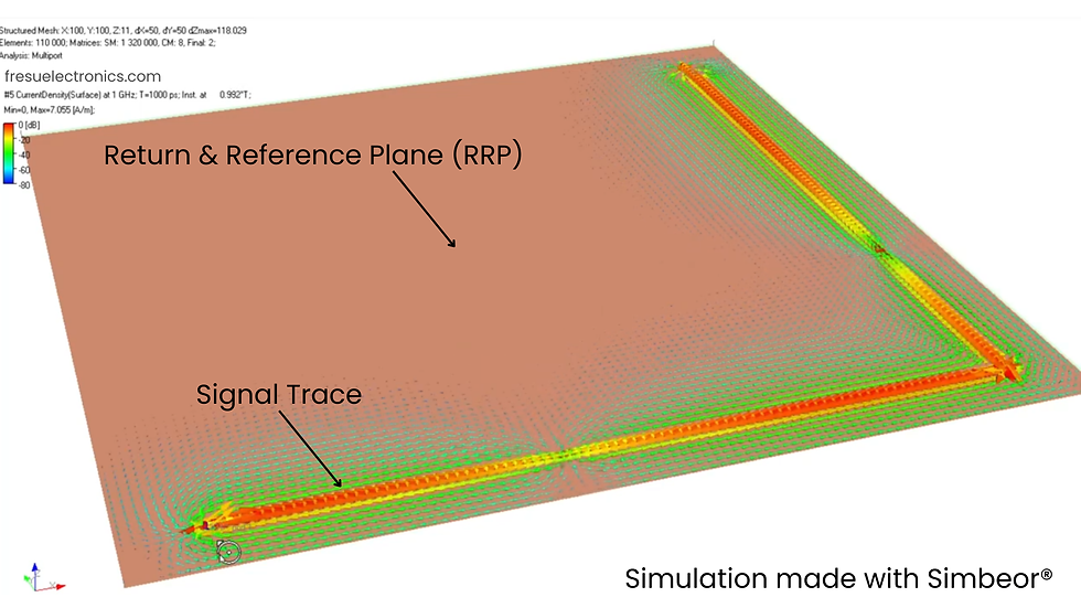
High-Speed Signal (1 GHz)
In contrast, high-frequency signals, such as those at 1 GHz, exhibit more pronounced behavior. As frequency increases, the reactive component of impedance becomes dominant due to inductance. To minimize this inductive effect, the return current flows as close as possible to the signal trace, following a path that significantly reduces reactance.
Understanding Current Loops
Current always flows in loops, meaning each signal trace has a corresponding return path. The current travels from the signal trace, through the return plane, and back to the source. Contrary to common misconceptions, the forward and return current processes occur simultaneously as the signal propagates. The forward current does not need to reach the load before the return current begins. This simultaneous flow is facilitated by displacement current (a changing electric field over time, such as the signal wavefront) which bridges the current loop during propagation. As signal frequency increases, the return current forms a tighter loop, staying closer to the signal trace. This distinction between low- and high-frequency signals is critical for PCB layout design, as the layout must accommodate these behavioral changes.

💡 Design Recommendation: The return reference plane should be placed on an adjacent layer, as close as possible to the signal layer, to minimize loop inductance and ensure signal integrity.
Challenges with Mixed-Frequency Signals
When signals operating at different frequencies are routed in close proximity on a PCB, several design challenges can emerge due to the interaction of their return currents. For example, consider a scenario where a high-frequency signal (e.g., 1 GHz) and a low-frequency signal (e.g., 10 kHz) are placed adjacent to each other on the same layer. While the high-frequency signal’s return current tightly follows its trace to minimize inductance, the low-frequency signal’s return current, although already influenced by inductance at 10 kHz, may still seek alternative paths if the return plane’s impedance varies locally.
This behavior can lead the low-frequency return current to deviate, flowing around the high-frequency signal’s trace in an attempt to find a lower-impedance path. Such deviations create unintended current loops, increasing the risk of electromagnetic coupling between the signals. This coupling manifests as crosstalk, where energy from one signal induces noise in the other, potentially corrupting data or degrading signal quality. Additionally, the irregular return path can cause ground bounce, where fluctuations in the reference plane’s voltage disrupt the stability of other signals sharing the same plane. These issues are particularly problematic in mixed-signal designs, such as those combining analog and digital circuits, where low-frequency analog signals might coexist with high-speed digital signals.
To mitigate these challenges, careful PCB layout planning is essential. Strategies include increasing the physical separation between high- and low-frequency traces (not splitting planes!), and proper stackup design, ensuring each signal layer has an adjacent reference plane, which also helps maintain consistent return paths and reduces the likelihood of unwanted coupling.
Impact of Trace Length on Return Currents
The length of the trace also influences return current behavior. For a 1 GHz signal, the return current remains closely coupled with the trace, maintaining the closest path back to the signal trace.

At 10 kHz, however, the return current spreads out more across the return plane due to the lower frequency signal’s reduced dependence on inductance. This results in the return current occupying a larger area of the return reference plane, as indicated by small green arrows in the simulation.
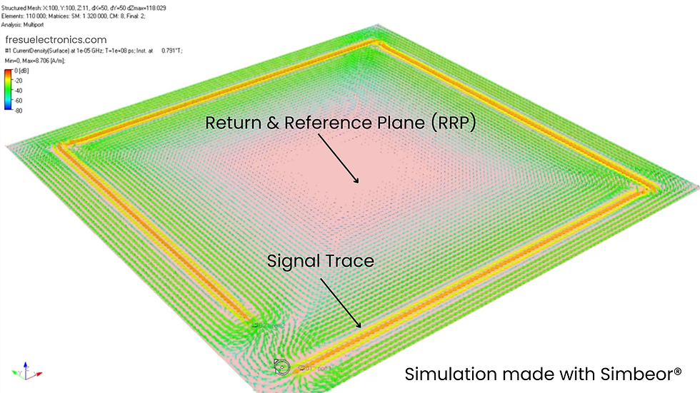
In the case of the 10 kHz signal, a portion of the return current still follows the path of shortest distance to the source. However, the inductive effect ensures that the majority of the return current remains close to the signal trace, independent of the length of the trace.
Effects of Return Plane Discontinuities
Splits in the Return Plane
Introducing a split or cut into the return reference plane significantly alters the behavior of return currents. In this scenario, a signal trace is routed across a split in the return plane, as shown in the image below. This represents a common design mistake in PCBs, where a signal trace on the top layer crosses over a discontinuity in the return plane below. Such splits are often introduced in an attempt to separate different circuit domains, like analog and digital sections, but they disrupt the return current path and lead to significant issues.

When a signal trace crosses one of these splits, the return current cannot flow directly beneath the trace as it would with a continuous plane. Instead, it must find an alternative path, leading to increased impedance and a larger current loop. Enlarging the current loop is the number one cause of radiated emissions since the emissions are proportional to the area enclosed by the whole current loop. For more details, see the Radiated Emissions - EMI Control guide here:
To illustrate this, a simulation demonstrates the behavior of return current when a trace crosses a split in the plane, highlighting the effects of such discontinuities and emphasizing the importance of maintaining uninterrupted return paths in PCB layouts.
Low-Frequency Signals Across a Split
For a 10 kHz signal, the return current is forced to take an indirect path around the discontinuity, creating a large return current loop, as indicated by green and yellow arrows in the simulation.

This large loop increases electromagnetic fields and can interact with other signals sharing the same return layer, leading to signal integrity and EMI issues. The signal traces on the top layer are particularly affected by the return current below.
High-Frequency Signals Across a Split
For a 1 GHz signal, the return path initially stays close to the trace but is disrupted upon encountering the split. The return current then diverts, potentially causing reflections and resonance within the cavity (essentially, the gap between the planes) as it attempts to flow back to the source. This resonance amplifies interference, underscoring the challenges posed by plane cuts.

These effects contribute to challenges in both signal integrity and EMC. The uncontained energy can effectively turn the system into an antenna, leading to further EMI complications and inefficiencies. Maintaining the integrity of the reference plane is essential to avoid such issues. If you are interested in learning more about how this type of simulation can help you find issues in your designs, click here to watch the full masterclass.
💡Design Recommendation: Avoid cuts, splits, or any interruptions in the return plane, especially when separating analog and digital signals. Using a separate "ground" is not recommended.
Best Practices for PCB Design and EMI Mitigation
Effective PCB design requires careful attention to return current behavior, as demonstrated throughout this article. For instance, even at 10 kHz, inductance causes the return current to follow the signal trace, a behavior that becomes more pronounced at 1 GHz. Longer traces at 10 kHz show a slight broadening of the return current, while mixed-frequency signals can lead to crosstalk if not properly managed. Additionally, routing a signal trace over a split in the return plane—a frequent design error—disrupts the current path, increasing EMI.
To ensure optimal performance and minimize EMI, consider the following guidelines:
Maintain Continuous Return Planes: Each signal layer should have an adjacent, uninterrupted return plane to provide a low-impedance path, avoiding issues like those caused by splits in the return plane.
Minimize Loop Inductance: Position return planes close to signal layers to reduce inductance, ensuring tight coupling of return currents, as observed at both 10 kHz and 1 GHz.
Manage Mixed-Frequency Signals: Ensure sufficient distance between high- and low-frequency traces to reduce interference. While routing them on different layers can help, avoid splitting the return plane with cuts between analog and digital sections, as this disrupts the return path and increases EMI.
Avoid Routing Over Plane Splits: Avid routing traces over discontinuities in the return plane, as this leads to larger current loops, resonances and EMI, as seen in the simulations.
Connect to Reference Voltage: Use the reference voltage for the return plane to ensure stability, avoiding power plane connections that may introduce noise. Further resources on this topic are available for deeper exploration.
Failure to meet this condition can compromise the return current, potentially leading to signal integrity issues and EMC problems.
Conclusion
Understanding how return currents behave at different frequencies is critical for designing high-performance PCBs. Low-frequency signals spread across the return plane, while high-frequency signals couple tightly to the signal trace. Discontinuities, such as splits in the return plane, disrupt these paths, leading to signal integrity and EMC challenges. By adhering to best practices—such as maintaining continuous return planes and simulating designs—engineers can create reliable, efficient PCBs that meet stringent performance and compliance requirements. At Fresu Electronics, we are committed to supporting engineers in mastering these design principles. Explore our courses and EMI control guides to enhance your skills.


Comments