Power Planes as Return Reference Planes in PCB Design: Challenges and Solutions in Multilayer Stackups
- Dario Fresu

- Apr 27, 2025
- 6 min read

Introduction
In the design of printed circuit boards (PCBs), the stackup configuration is a critical factor that influences signal integrity, electromagnetic interference (EMI), and overall system performance. A common practice, particularly in cost-constrained designs, is to use power planes as return reference planes (RRPs) for signal layers. This approach is frequently employed in the widely adopted four-layer stackup, consisting of a signal layer, a power plane, a ground plane, and another signal layer. While this configuration is economical, it introduces complexities in managing return currents, especially in multilayer stackups where power and ground planes are often separated by multiple layers. This article examines the implications of using power planes as RRPs, with a particular focus on multilayer stackups, and provides practical solutions to ensure robust signal integrity and EMI performance.
The Role of Return Reference Planes
Return reference planes provide a low-impedance path for the return current of a signal to complete its circuit back to the source. For optimal signal integrity, the RRP should be a solid ground plane located directly adjacent to the signal layer, minimizing loop inductance and ensuring clean signal transmission. In a typical four-layer stackup—signal, power, ground, signal—the top signal layer references the power plane as its RRP. This configuration deviates from the ideal scenario, as the power plane operates at a different DC potential (e.g., 3.3V or 5V) than the ground plane, creating challenges for return current paths.
In multilayer stackups, which are common in high-speed, high-density designs, the complexity increases. These stackups, often comprising six, eight, or more layers, may position power planes several layers away from ground planes, exacerbating issues related to return current coupling and impedance. Understanding these challenges is essential for designing reliable PCBs, particularly as signal speeds continue to rise.
Challenges of Using Power Planes as Return Reference Planes
When a signal layer references a power plane, the return current must find a path to couple to the ground plane to close the circuit. Since power and ground planes are DC-disconnected, this coupling occurs through displacement current, which flows through the interplane capacitance between the planes. This process introduces several challenges, which are amplified in multilayer stackups.
Displacement Current and Interplane Impedance
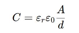
Displacement current relies on the capacitance between the power and ground planes, which is determined by the formula:

Where ( C ) is the capacitance, ( εr) is the relative permittivity of the dielectric, ( ε0 ) is the permittivity of free space, ( A ) is the overlapping area of the planes, and ( d ) is the distance between the planes. This capacitance facilitates high-frequency AC coupling, allowing return currents to transition between planes. However, the impedance associated with this capacitance, given by ( Z = 1/ (2 π f C)), where ( f ) is the frequency, introduces a voltage drop when current flows through it. This voltage drop manifests as noise across the board, potentially degrading signal quality and increasing EMI.
In a four-layer stackup, the power and ground planes are typically separated by a dielectric layer, which may range from 4–8 mils in high-performance designs to 20–40 mils in standard, cost-optimized boards. Thinner dielectrics result in higher interplane capacitance and lower impedance, improving signal integrity, while thicker dielectrics reduce capacitance and increase impedance, posing challenges for high-speed signals.
Loop Inductance and Signal Integrity
The distance between the signal layer, the power plane as its reference plane, and the ground plane directly affects the loop inductance of the return path. In multilayer stackups, a power plane located far from the ground plane creates a larger loop area for the return current, increasing inductance. High loop inductance can lead to ground bounce, where rapid current changes induce voltage spikes, and crosstalk, where signals couple to adjacent traces. For high-speed interfaces such as DDR, PCIe, or USB, these effects can cause timing errors, data corruption, and reduced system reliability.
Frequency Limitations of Decoupling Capacitors
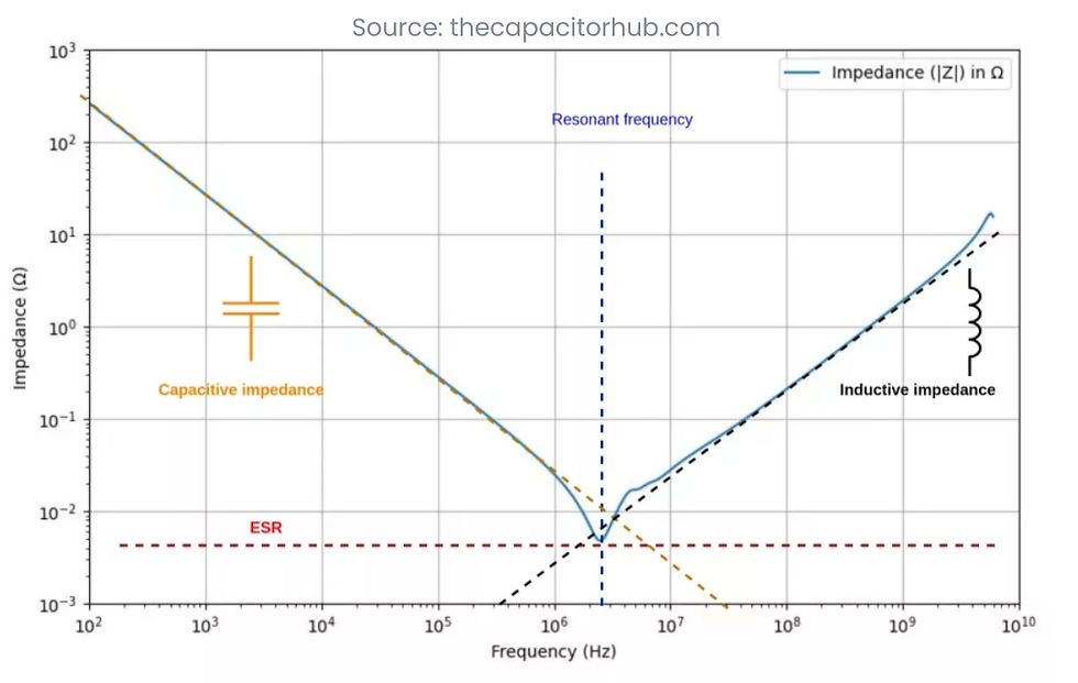
A common mitigation strategy is to use decoupling capacitors between power and ground planes to provide a low-impedance path for return currents at high frequencies. However, capacitors have an impedance profile that varies with frequency due to their parasitic inductance. At low frequencies, capacitors effectively bypass the interplane impedance, but above a certain frequency (typically in the MHz range), their impedance increases, reducing their effectiveness. In multilayer stackups, the greater separation between planes exacerbates this issue, as the interplane capacitance is less capable of supporting return currents at high frequencies.

Return Path Discontinuities in Multilayer PCB Designs
In multilayer stackups, signals frequently transition between layers using vias, which may cross multiple reference planes. If a signal references a power plane on one layer and a ground plane on another, the return current must jump between these planes, typically through decoupling capacitors or interplane capacitance. The farther the power and ground planes are, the higher the impedance of this transition, leading to return path discontinuities. These discontinuities cause signal reflections, increased noise, and elevated EMI, particularly in high-speed designs where signal edges are sharp.
Multilayer Stackups: A Closer Look
Multilayer stackups are designed to accommodate complex routing, multiple power domains, and high-speed signals, but they often prioritize routing density over ideal plane placement. A typical eight-layer stackup might be configured as follows:
Layer 1: Signal
Layer 2: Ground
Layer 3: Signal
Layer 4: Signal
Layer 5: Power
Layer 6: Signal
Layer 7: Ground
Layer 8: Signal
In this stackup, the power plane on Layer 5 is separated from the ground planes on Layers 2 and 7 by multiple signal layers and dielectric layers. This configuration is common in designs where cost or layer count constraints limit the number of ground planes or dictate plane placement. However, it amplifies the challenges of using power planes as reference planes, as the increased interplane distance reduces capacitance and increases impedance.
For example, if a signal on Layer 6 references the power plane on Layer 5, the return current must couple to the ground plane on Layer 7 or Layer 2. The larger separation (e.g., 15–20 mils) results in low interplane capacitance, high impedance, and significant voltage drops, which can radiate as EMI or couple noise into other signals. Additionally, via transitions between layers further complicate the return path, as the current must navigate through capacitors or stitching vias to reach the ground plane.
Solutions for Effective Design
To address the challenges associated with using power planes as RRPs in multilayer stackups, designers can implement various strategies to maintain signal integrity and reduce EMI. These approaches emphasize optimizing plane placement, improving decoupling, and managing return paths.
The primary guideline is to ensure that each signal or power plane is adjacent to a return and reference plane (also called ground). This plane must be free of splits, cuts, or gaps to provide a continuous reference for the signals.
Optimize Plane Placement
Using the power planes as both return and reference, with the power and ground planes as adjacent pairs, is the second most effective technique and is necessary for reducing interplane impedance. In an eight-layer stackup, a more optimal configuration might be:
Layer 1: Signal
Layer 2: Ground
Layer 3: Power
Layer 4: Signal
Layer 5: Signal
Layer 6: Power
Layer 7: Ground
Layer 8: Signal
This stackup places power and ground planes adjacent to each other (Layers 2–3 and 6–7), maximizing interplane capacitance and minimizing impedance. A thinner dielectric (e.g., 4 mils) between these planes further increases capacitance, reducing the voltage drop caused by displacement current. While this approach may increase fabrication costs, it significantly improves signal integrity and EMI performance. In this setup, all the planes, including the power planes, are solid, with no splits, cuts, or gaps. This ensures that signals referencing these planes have a nearby and continuous return and reference path adjacent to them.
Manage Return Path Discontinuities
To minimize the impact of via transitions and plane changes:
Include return vias near signal vias to provide a low-impedance path for return currents. These vias should connect to the appropriate return and reference plane.
Use back-drilled vias or blind/buried vias to eliminate stub effects, which can resonate and degrade high-speed signals.
With performance critical designs, make sure to simulate return paths using tools like 3D field solvers such as SIMBEOR® to identify and address discontinuities before fabrication.
Conclusion
Using power planes as return reference planes in PCB design is a common practice, but it introduces significant challenges, particularly in multilayer stackups where power and ground planes are often separated by multiple layers. The increased interplane distance reduces capacitance, raises impedance, and amplifies voltage drops, leading to signal integrity issues and EMI. By optimizing plane placement, managing return paths, and leveraging simulation tools, designers can mitigate these challenges and achieve reliable performance. Careful stackup design and adherence to best practices are essential for balancing cost, performance, and reliability in modern PCB designs. At Fresu Electronics, we are dedicated to helping engineers grasp and implement best design practices from the outset. If you're interested in enhancing your skills, we invite you to explore our courses and EMI control guides.


Comments