

Fundamentals of PCB Design For EMC & Low EMI
- Dario Fresu

- Nov 13, 2024
- 9 min read
Updated: Feb 24, 2025
CLICK THE PLAY BUTTON TO WATCH THE LESSON.
Action list:
In this article, we are going to explore the fundamental concepts necessary to understand Printed Circuit Board design for passing EMC.
In electronics or electrical circuits classes, we have learned to design circuits according to the water through the pipes analogy. Although those analogies are helpful for simplifying circuit design, when we discuss printed circuit board design, we have to take one step back and consider the true fundamentals, the Maxwell's equations.

Before you decide to run away from this lesson, what we need at this point as designers is not so much to go back and understand the math of the equations, but rather to understand the principles behind them, in this way, we can visualize these effects and build boards that excel in terms of reliability, immunity to disturbances, and compatibility with other systems.
🔓 This means that we ensure that our system can work with other nearby devices and systems, without disrupting its normal operation, or the normal operation of other devices.
To be able to do that, we need to visualize the electromagnetic fields in a printed circuit board trace, at least at a basic level. Let's now take a simple example of a printed circuit board and analyze how it can helps us visualize the fields. In this picture, we can see a cross section view of a double layer printed circuit board.
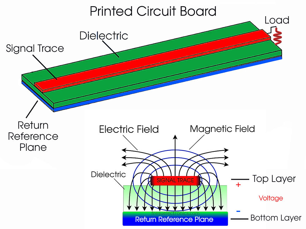
The top layer is represented by the red colored signal trace, and the bottom trace for the reference plane is represented by the blue color. Also, to complete the picture, we have the dielectric layer (in green), which is placed between the signal layer on the top, and the return reference plane on the bottom layer.
From this picture, we can observe that different phenomena are occurring. The first thing we notice is the presence of fields. The electric field described from the black arrows and the magnetic field described by the blue circles. Of course, this assumes that a signal is present on the signal trace. Here, we can observe that the electric field lines are radiating from the signal trace.

Their direction changes depending on the position of the trace in relation to the return reference plane. In this PCB, where the return reference plane is close to a signal trace, the electric fields generated by the signal trace are naturally drawn towards this plane and terminate there. On the top side of the signal trace instead, where there is no return reference plane, the electric field lines from the signal trace are partially uncontained.
Why is this important for us?
Without a return reference plane (RRP) close to the signal trace, electric fields can extend further, grow larger, and may interact with unintended parts of the circuit, or external environments, potentially leading to electromagnetic interference issues. This is why return reference planes are critical in PCB design, to ensure controlled propagation of electric and magnetic fields and to minimize interference.
Many of the problems we encounter during EMC tests, in fact, arise from poorly designed layouts where the fields are not well contained and extend further disrupting the operation of other devices or components.
🔓 If you think about it, during EMC tests such as radiated and conducted tests, what we are measuring is the energy level of these fields.
The quickest way to encounter EMC issues, in fact, is to remove the return reference plane from the vicinity of the signal trace. This allows the fields to expand and create disruptions in undesired locations. In simple terms, when this is done, the electric fields are no longer confined and can grow larger, possibly reaching other devices or component structures. When this occurs, the return current loops, formed through parasitic paths, will also grow, causing an increase in electromagnetic fields that can further disrupt operations.
The concept of Return Reference Plane (RRP)
The Return Reference Plane gets its name for two reasons.
Firstly, it serves as the return path for the signal traces. This means that the return current generated by the signal will flow back to the source through the Return Reference Plane (RRP), completing the current loop.
Secondly, it earns this name because it provides the reference potential for the signal trace. In other words, it offers the signal a reference for its electric fields.
🔓Before we proceed to the next steps, I'd like to point out that I haven't referred to the return reference plane as "ground". This is because, more often than not, the term ground is misused and wrongly used to describe the location where current sinks.
What we've explained so far should also address why having the return reference plane adjacent to the signal trace in the stackup is the optimal choice.
Firstly, it's because if the fields generated from different signals are not separated, they could interfere with one another.
Secondly, it's due to the importance of completing the current loops. If the current loops are not closed, the current cannot flow.
These loops can be completed through two types of current:
Conduction current, which includes signal (or forward) current, and return current.
Displacement current,
or a combination of both. You can find a more detailed explanation of these concepts in the lesson on "How Signals Propagate in a Printed Circuit Board (PCB)".
Power Plane are not good as Return and Reference Planes
What happens when we introduce between the signal trace and the return reference plane another plane with a voltage different than the driving voltage?

For the return current, the voltage of the return plane doesn't really matter. What matters is the path of least impedance. Therefore, the current will still flow through the power plane. The problem now is returning to the source to complete the current loop.
Since the power plane is not DC connected to the return reference plane (because this would create a short-circuit), the return current will still need to find a way to complete the loop and return to the source. Only now, there will be an additional impedance that the signals see between the power layer and the return reference layer.
💡 By the way, If you would like to master EMC/EMI design, we have a new training program here:
There, you’ll find details on how to apply for one of our exclusive programs designed to help you achieve that goal.
In this case, the return current will have to reach the reference plane not through conduction current, but via the displacement current, because the planes are not connected to the same DC voltage.
This means that there will be an impedance between the two planes. If we have an impedance, it means that we will have a voltage drop, which can cause noise and create problems such as "ground bounce."
🔓Ground bounce is essentially a voltage fluctuation in the Return and Reference plane of a circuit.
We won't go into too much detail in this article. The only thing we really need to know is that the best way for us to minimize noise and electromagnetic interferences is to have the return reference plane adjacent to the signal trace.
Signal transitioning layers
This brings us to the next point. What happens when the signal transitions from the top layer to the bottom layer?

If we have layer 2 and layer 3 at the same voltage, and we use return stitching vias to connect the planes together, keeping them equipped potential, the return current will utilize the stitching vias to return to the source, and there won't be any problems.
However, if layer two and layer three have different voltages, as in the case we previously analyzed, we cannot add stitching via because the planes have different voltages.
In this scenario, the signal would have to traverse the impedance between the two planes until it finds its way back to the driving source.
This can lead to voltage drops between the planes (depending on the signals), potentially causing noise in the circuit.
Using decoupling capacitors for signals transitioning layers.
The problem persists even if we decide to use capacitors to connect the two planes.
The issue with decoupling capacitors is that the impedance of the capacitors changes with frequency, and is only effective for signals at low frequencies.

This is why we are going to use the stack up configuration, where we have a return reference plane next to the signal layer. We are also going to use stitching vias to connect the planes, and add a return via next to the signal layers, each time the signals cross from one layer to the other.
It's also important to note here that the planes should be designed to have the lowest possible impedance for the signal return current to flow back to the source. The most effective way to achieve this is by using a plane that doesn't have splits, cuts or other irregularities that would alter the impedance of the plane.
How return current changes based on frequency
Let's now discuss another important point: differences in return current. This is one of the reasons many application notes recommend separating the analog and digital sections on the board, yet it remains one of the most misunderstood concepts.
As we know from the fundamentals of electronics, impedance Z is frequency dependent.

This is because we have the real part of the impedance, which is resistance, and the imaginary part of the impedance, which is called reactance.

The reactance term in the impedance equation, which includes inductive reactance and capacitive reactance, makes it frequency dependent. This is because both inductive reactance and capacitive reactance change based on frequency.

For low frequency or DC signals, the return current spreads out over the return reference plane, seeking the path of least resistance. This spreading allows the return current to take a more distributed path back to the source. In contrast, for high frequency signals, the return current path is much more localized, and It tends to follow directly underneath the signal trace.

This phenomenon is explained by the skin effect, and the principle of minimizing the loop area, between the signal trace and its return path to reduce the total inductance and, consequently, the reactance. The high frequency return current effectively follows the path of least inductance, rather than the path of least resistance.
Digital signals characterized by the sharp transitions inherently contain a broad spectrum of frequency components due to their harmonic content. This includes a fundamental frequency and its harmonics at integer multiples of the fundamental frequency. According to Fourier analysis, any square or sharp edged signal can be decomposed into a series of sine waves at different frequencies.

The faster the edge rate, meaning the sharper the transition from low to high or high to low, the higher the frequency of the harmonics that compose the signal. These harmonics mean that even a digital signal, which might be considered low frequency, based on its fundamental frequency, can have high frequency components.
High frequency signals, therefore, can generate significant amounts of electromagnetic interference that can couple into low frequency signal lines, causing noise and potentially corrupting the signals, called crosstalk.
Crosstalk is an unwanted coupling between signal paths, which can be particularly problematic when high frequency signals induce disturbances in low frequency or sensitive analog signal paths.
High frequency signals have a higher tendency to couple with adjacent traces due to their electromagnetic fields. By physically separating these signals, the risk of crosstalk is minimized, ensuring that the low frequency signals remain clean and undisturbed.
This is especially critical for analog signals, which are susceptible to even small levels of noise. Separating these signals on the PCB layout helps to reduce the noise coupling from high frequency digital circuits to low frequency and analog circuits.
🔓 Please note that we have never mentioned separating the return reference planes as certain application notes may suggest.
Avoiding this bad practice is important as it can lead to more issues than benefits.
Conclusion
I hope this lesson helps you identify some potential pitfalls in circuit design and empowers you to avoid them altogether. When someone begins their journey in PCB design, the theoretical knowledge gained in classical electrical engineering classes does not always translate seamlessly into practical PCB layout practices. This often leaves hardware designers in a challenging position, learning through trial and error.
At fresuelectronics.com , our primary goal is to help you circumvent the pain associated with this steep learning curve. We believe that by sharing this guide, along with the courses, materials, and programs we offer, we can assist you in navigating the complexities of PCB design. Our aim is to support you on your path to mastering this field, ensuring that you have the tools and knowledge necessary to succeed.
If you would like to master EMC/EMI design, we have a new training program here:
There, you’ll find details on how to apply for one of our exclusive programs designed to help you achieve that goal.


Comments